


68
CHAPTER 3 CPU
■ Memory access mode selection operation
Only the single-chip mode can be selected.
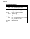
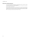
Table 3.8-2 "Mode pin and mode data" lists the mode pin and mode data options.
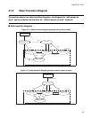
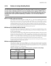
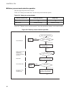
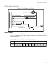
Figure 3.8-2 "Memory access selection operation" shows the operation for memory access mode selection.
Figure 3.8-2 Memory access selection operation
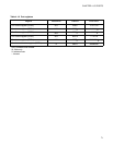
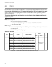
Table 3.8-2 Mode pins and mode data
Memory access mode Mode pin (MODA) Mode data
Single-chip mode V
SS
00
H
Other modes Prohibited settings Prohibited settings
Check mode pin
Delay for wake-up from
(external reset or
reset source
oscillation stabilization
delay time)
Mode fetch
Check mode data
Set I/O pin functions
for program
execution (RUN)
Reset source generated
Mode pin (MODA)
Read mode data from
internal ROM
I/O pins are high
impedance
Reset active?
Fetch mode data and reset
vector from internal ROM.
Mode data
Single-chip mode (00
H
)
Set I/O pins to input or output
depending on their respective port
data direction registers (DDR),
etc.
I/O pins are available as
ports
Single-chip mode
VSS
Prohibited
setting
Other
Prohibited
setting
Other