


12
CHAPTER 1 OVERVIEW
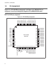
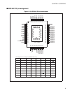
1.7 I/O Pins and Pin Functions
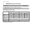
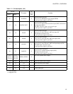
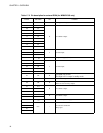
Table 1.7-1 "Pin description" and Table 1.7-2 "Pin description for external ROM (for
MB89PV950 only)" list the MB89950/950A series I/O pins and their functions. Table 1.7-3
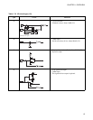
"I/O circuit type" lists the I/O circuit types.
The letter in the "I/O circuit type" column in Table 1.7-1 "Pin description" refer to the
letter in the "Type" column Table 1.7-3 "I/O circuit type".
■ I/O pins and pin functions
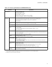
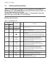
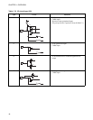
Table 1.7-1 Pin description (1/2)
Pin no.
Pin name
I/O
circuit
type
Function
LQFP
*1
MQFP
*2
22 23 X0
A Clock oscillator pins.
23 24 X1
21 22 MODA B
Operation mode selection pin.
This pin is connected directly to V
SS
with pull-down resistor.
19 20 RST C
Reset I/O pin.
This pin consists of an N-ch open-drain output with a pull-up
resistor and hysteresis input. A "LOW" level is output from this
pin. A "LOW" voltage on this port generates a RESET condition.
48 to 41 49 to 42
P00/SEG20
to
P07/SEG27
D
N-channel open-drain type general-purpose I/O ports.
Also serve as LCD controller/driver segment outputs.
Switching between port output and segment driver output is
performed by the mask option.
40 to 33 41 to 34
P10/SEG28
to
P17/SEG35
D
N-channel open-drain type general-purpose I/O ports.
Also serve as LCD controller/driver segment outputs.
Switching between port output and segment driver output is
performed by the mask option.
32 to 27 33 to 28
P20/SEG36
to
P25/SEG41
D
N-channel open-drain type general-purpose I/O ports.
Also serve as LCD controller/driver segment outputs.
Switching between port output and segment driver output is
performed by the mask option.
14 to 13 15 to 14 P30 to P31 F N-channel open-drain type general-purpose I/O ports.
12 to 11 13 to 12
P32/V1 to
P33/V2
H
N-channel open-drain type general-purpose I/O ports.
Also serve as LCD controller/driver power supply.
15 16 P40 E
General-purpose I/O port.
A pull-up resistor option is provided.