


245
CHAPTER 12 LCD CONTROLLER/DRIVER
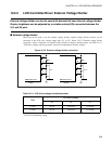
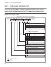
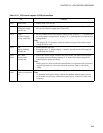
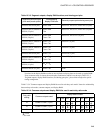
Table 12.3-1 LCD control register (LCDR) bit functions
Bit Function
Bit 7 Reserved bit • Always write "0" to this bit.
Bit 6 PSEL:
LCD power supply
selection bit
• Selects P32/V1 and P33/V2 to function either as N-ch open-drain I/O ports (P32,
P33) or as LCD power supply pins (V1 and V2).
Bit 5 VSEL:
LCD drive supply
voltage control bit
• This bit controls the use of the internal voltage divider. Writing a "1" to it enables the
use of the internal voltage divider. Writing a "0" to it disables the use of the internal
voltage divider.
Note:
This bit must be "0" in order to isolate the internal voltage divider when external
voltage divider is used.
Bit 4 BK:
Display blanking
selection bit
• Blanks/unblanks the LCD.
• Setting this bit to "1" (blank) outputs a "deselect" waveform to the LCD segments
(which blanks the display).
Bit 3
Bit 2
MS1, MS0:
Display mode
selection bits
• Selects one of three output waveform duty ratio modes. The mode selected affects
the common pins used. Setting both bits to "0" turns off the display (stops LCD
controller/driver display operation).
Note:
Before going to a mode in which the selected frame cycle generate clock oscillator is
stopped (stop mode, etc.), these bits should be written to "00
B
" to turn off the
display.
Bit 1
Bit 0
FP1, FP0:
Frame cycle selection
bits
• These bits select one of four LCD frame cycles.
Note:
To determine this register setting, calculate the optimum frame frequency for the
LCD module you are using. Note that the frame cycle is a function of main clock
frequency.