


173
CHAPTER 9 8-BIT SERIAL I/O
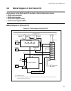
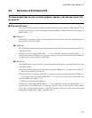
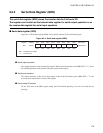
9.3 Structure of 8-bit Serial I/O
This section describes the pins, pin block diagram, registers, and interrupt source of 8-
bit serial I/O.
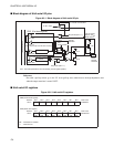
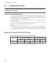
■ 8-bit serial I/O pins
8-bit serial I/O uses the P43/SI, P44/SO, and P45/SCK. The pins are also used as UART I/O pins. To use
the pins as serial I/O pins, set the UART/SIO selection bit RSEL of UART serial mode control register 2
(SMC2: RSEL = "1").
●
P43/SI pin
The P43/SI pin can function either as a general-purpose I/O port (P43) or as the serial data input (hysteresis
input) for 8-bit serial I/O or UART.
●
P44/SO pin
The P44/SO pin can function either as a general-purpose I/O port (P44) or as the serial data output for 8-bit
serial I/O or UART.
Enabling serial data output (SMR: SOE = "1" and UART/SIO selection bit SMC2: RSEL = "1")
automatically sets the P44/SO pin as an output pin, regardless of the port data direction register (DDR4: bit
4) value, and sets the pin to function as the SO pin.
●
P45/SCK pin
The P45/SCK pin can function either as a general-purpose I/O port (P45) or as the shift clock I/O for 8-bit
serial I/O or UART.
Set P45/SCK pin as an input port in the data direction register (DDR4: bit 5 = "0") when using as SCK pin.
• When using as the shift clock input pin
When using SCK as an input pin, set the pin as an input port in the port data direction register (DDR4: bit 5
= "0") and disable shift clock output (SMR: SCKE = "0"). In this case, always select external shift clock
operation (SMR: CKS1, CKS0 = "11
B
").
• When using as the shift clock output pin
Enabling shift clock output (SMR: SCKE = "1" and UART/SIO selection bit SMC2: RSEL = "1")
automatically sets the P45/SCK pin as an output pin, regardless of the port data direction register (DDR4:
bit 5) value, and sets the pin to function as the SCK output pin. In this case, always select internal shift
clock operation (SMR: CKS1, CKS0 = other than "11
B
").