


243
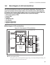
CHAPTER 12 LCD CONTROLLER/DRIVER
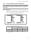
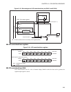
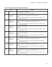
Figure 12.3-3 Block diagram of LCD controller/driver pin (P32/V1 and P33/V2)
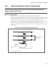
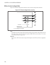
■ LCD controller/driver registers
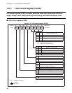
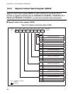
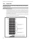
Figure 12.3-4 LCD controller/driver registers
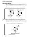
■ LCD controller/driver RAM
LCD controller/driver has 42 x 4-bit of internal display RAM in which the data used to generate the
segment output signals is stored.
PDR (Port data register)
Internal data bus
PDR read (for bit manipulation instructions)
Output latch
PDR write
Pin
N-ch
N-ch P-ch
Stop mode (SPL = 1)
SPL: Pin state specification bit in the standby control register (STBC)
PDR read
Stop mode (SPL = 1)
PSEL bit of LCDR register
V1 or V2
P32/V1
P33/V2
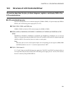
Address Bit 7 Bit 6 Bit 5 Bit 4 Bit 3 Bit 2 Bit 1 Bit 0 Initial value
0079
H
RESV PSEL VSEL BK MS1 MS0 FP1 FP0 -0010000
B
R/W R/W R/W R/W R/W R/W R/W R/W
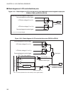
Address Bit 7 Bit 6 Bit 5 Bit 4 Bit 3 Bit 2 Bit 1 Bit 0 Initial value
007A
H SEG15 SEG14 SEG13 SEG12 SEG11 SEG10 SEG00 -0000000B
R/W R/W R/W R/W R/W R/W R/W
R/W : Readable and writable
: Unused
LCDR (LCD control register)
SEGR (Segment output select register)