


53
CHAPTER 3 CPU
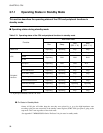
3.6.2 Clock Controller
The clock controller contains the following four blocks:
• Main clock oscillator
• Clock controller
• Oscillation stabilization delay time selector
• Standby control register (STBC)
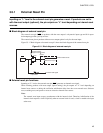
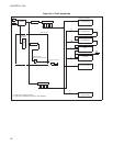
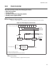
■ Block diagram of clock controller
Figure 3.6-4 "Block diagram of clock controller" shows the block diagram of the clock controller.
Figure 3.6-4 Block diagram of clock controller
●
Main clock oscillator
The main clock oscillator is stopped in main stop mode.
Pin state
Stop mode
Sleep mode
Clock for
Main clock
oscillator
Enable
Clock
controller
Stop of supply to the CPU
timebase timer
STBC STP SLP SPL RST — — — —
Divid e-by-2
Divide-by-4
Clock supply
to CPU
1 tinst
2
14
/FCH
2
18
/FCH
From timebase timer
Oscillation stabiliza-
tion delay time
selector (optional)
Standby control register (STBC)
F
CH
Mask option
FCH: Main clock oscillation frequency
t
inst: Instruction cycle (divide-by-four main clock oscillation)