


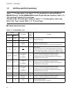

13
CHAPTER 1 OVERVIEW
16 17 P41/PWM E
General-purpose I/O port.
Also serves as PWM timer toggle output (PWM).
A pull-up resistor option is provided.
17 18 P42/PWC/INT1 E
General-purpose I/O port.
Also serves as pulse-width count timer input (PWC) and external
interrupt input (INT1).
The PWC and INT1 inputs are hysteresis type.
A pull-up resistor option is provided.
18 19 P43/SI E
General-purpose I/O port.
Also serves as serial I/O and UART data input (SI).
The SI input is hysteresis type.
A pull-up resistor option is provided.
20 21 P44/SO E
General-purpose I/O port.
Also serves as serial I/O and UART data output (SO).
A pull-up resistor option is provided.
25 26 P45/SCK E
General-purpose I/O port.
Also serves as serial I/O and UART clock input/output (SCK).
The SCK input is hysteresis type.
A pull-up resistor option is provided.
26 27 P46/INT0 E
General-purpose input port.
Also serves as external interrupt input (INT0).
The input is hysteresis type.
A pull-up resistor option is provided.
5 to 1
64 to 57
55 to 49
6 to 1
64 to 58
56 to 50
SEG0 to SEG19 G
For LCD segment driver outputs.
9 to 6 10 to 7 COM0 to COM3 G For LCD common driver outputs.
10 11 V3 - For LCD driver power supply.
56 57
V
CC
-
Power pin.
24 25
V
SS
-
Power (GND) pin.
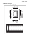
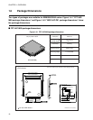
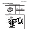
*1: FPT-64P-M09
*2: MQP-64C-P01
Table 1.7-1 Pin description (2/2)
Pin no.
Pin name
I/O
circuit
type
Function
LQFP
*1
MQFP
*2