


146
CHAPTER 8 PULSE WIDTH COUNT TIMER (PWC)
8.3 Structure of Pulse Width Count Timer
This section describes the pins, pin block diagram, registers, and interrupt source of
the pulse width count timer.
■ Pulse width count timer pin
The pulse width count timer uses the P42/PWC/INT1 pin. This pin can function either as CMOS general-
purpose I/O port (P42) or external interrupt (INT1), or as the measured pulse input (PWC).
PWC:
The pulse width measurement function measures the pulse widths input to this pin.
Set the pin as an input port in the port data direction register (DDR4: bit 2 = "0") when using as the
PWC pin for the pulse width measurement function.
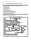
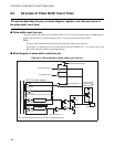
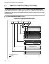
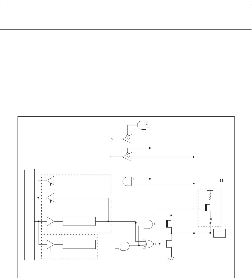
■ Block diagram of pulse width count timer pin
Figure 8.3-1 Block diagram of pulse width count timer pin
PDR (Port data register)
DDR
Internal data bus
PDR read
PDR read
Output latch
PDR write
DDR write
Pin
SPL: Pin state specification bit in the standby control register (STBC)
N-c
P42/PWC/INT1
h
Stop mode (SPL = 1)
To peripheral input
(Port data direction register)
P-ch
Pull-up resistor
Approx. 50 k
P-ch
(When Read-modify-write instruction executed)
Stop mode (SPL = 1)
To external interrupt
External interrupt enable
(Mask option)