


x
CHAPTER 11 EXTERNAL INTERRUPT CIRCUIT (EDGE) ............................................ 223
11.1 Overview of the External Interrupt Circuit ........................................................................................ 224
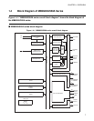
11.2 Block Diagram of the External Interrupt Circuit ................................................................................. 225
11.3 Structure of the External Interrupt Circuit ......................................................................................... 226
11.3.1 External Interrupt Control Register (EIC) ..................................................................................... 228
11.4 External Interrupt Circuit Interrupts ................................................................................................... 230
11.5 Operation of the External Interrupt Circuit ........................................................................................ 231
11.6 Program Example for the External Interrupt Circuit .......................................................................... 232
CHAPTER 12 LCD CONTROLLER/DRIVER .................................................................. 233
12.1 Overview of LCD Controller/Driver .................................................................................................. 234
12.2 Block Diagram of LCD Controller/Driver .......................................................................................... 235
12.2.1 LCD Controller/Driver Internal Voltage Divider ............................................................................ 237
12.2.2 LCD Controller/Driver External Voltage Divider ........................................................................... 239
12.3 Structure of LCD Controller/Driver .................................................................................................... 241
12.3.1 LCD Control Register (LCDR) ..................................................................................................... 244
12.3.2 Segment Output Select Register (SEGR) .................................................................................... 246
12.3.3 Display RAM ................................................................................................................................ 248
12.4 Operation of LCD Controller/Driver .................................................................................................. 250
12.4.1 Output Waveforms during LCD Controller/Driver Operation (1/2 Duty Ratio) ............................. 251
12.4.2 Output Waveforms during LCD Controller/Driver Operation (1/3 Duty Ratio) ............................. 254
12.4.3 Output Waveforms during LCD Controller/Driver Operation (1/4 Duty Ratio) ............................. 257
12.5 Program Example for LCD Controller/Driver .................................................................................... 260
APPENDIX ......................................................................................................................... 263
APPENDIX A I/O Map ................................................................................................................................ 264
APPENDIX B Overview of Instructions ....................................................................................................... 266
B.1 Overview of F
2
MC-8L Instructions ................................................................................................. 267
B.2 Addressing ..................................................................................................................................... 269
B.3 Special Instructions ........................................................................................................................ 274
B.4 Bit Manipulation Instructions (SETB, CLRB) .................................................................................. 278
B.5 F
2
MC-8L Instructions ..................................................................................................................... 279
B.6 Instruction map ............................................................................................................................... 286
APPENDIX C Mask Options ....................................................................................................................... 287
APPENDIX D Programming Specifications for One-Time PROM And EPROM Microcontroller ................ 289
D.1 Programming Specifications for One-time PROM and EPROM Microcontrollers .......................... 290
D.2 Programming Yield and Erasure .................................................................................................... 293
D.3 Programming to the EPROM with Piggyback/Evaluation Device ................................................... 294
APPENDIX E MB89950/950A Series Pin States ........................................................................................ 295
INDEX................................................................................................................................... 297