


203
CHAPTER 10 UART
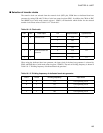
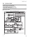
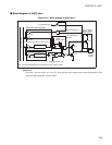
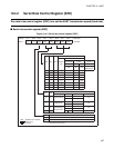
■ Block diagram of UART pins
Figure 10.3-1 Block diagram of UART pins
Reference:
Pins with a pull-up resistor go to the "H" level (pull-up state) rather than to the high-impedance state
when the output transistor is turned "OFF".
PDR (Port data register)
DDR
Internal data bus
PDR read
PDR read
Output latch
PDR write
DDR write
Pin
SPL: Pin state specification bit in the standby control register (STBC)
N-ch
Stop mode (SPL = 1)
To peripheral input
(Port data direction register)
UART output
UART
output enable
P-ch
Pull-up resistor
Approx. 50 k
P-ch
(When Read-modify-write instruction executed)
Stop mode (SPL = 1)
(Mask option)
P45/SCK
P44/SO
P43/SI
For P45/SCK and
For P45/SCK and P43/SI
P44/SO