


287
APPENDIX C Mask Options
APPENDIX C Mask Options
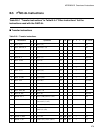
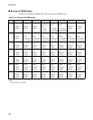
This appendix lists the mask options for the MB89950/950A series.
■ Mask options
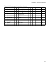
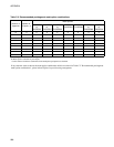
Table C-1 Mask options
No.
Part number
MB89951A
MB89953A
MB89P955 MB89PV950
Specifying procedure
Specify when
ordering mask
Set with EPROM
programmer
Setting not possible
1 Port pull-up resistor
P40 to P46
Can be selected for
each pin
Can be selected for
each pin
No pull-up resistor
2 Port/Segment output
P00 to P07, P10 to P17, P20 to P25
Can be selected for
every 8 to 1 pins
(*2)
Port/segment
output
(*3)
Port/segment
output
(*3)
3 Power-on reset
Power-on reset available
Power-on reset unavailable
Can be selected Can be selected Power-on reset
available
4 Selection of main clock oscillation
stabilization time (at 5 MHz)
(*1)
About 2
18
/F
CH
(about 52.4 ms)
About 2
14
/F
CH
(about 3.28 ms)
Can be selected Can be selected
2
18
/F
CH
5 Reset pin output
Reset output available
Reset output unavailable
Can be selected Can be selected Reset output
available
F
CH
: main clock oscillation frequency
*1: The main clock oscillation stabilization time is generated by dividing the main clock oscillation. Since the oscillation
cycle is unstable immediately after oscillation starts, the time in this table is only a guide.
*2: Port/segment output switching should be specified in the same manner as the port allocation set by the segment output
select register in the LCD controller described on Chapter 12 "LCD CONTROLLER/DRIVER".
*3: When these pins are used as ports, applied voltage should never be higher than V3.