


235
CHAPTER 12 LCD CONTROLLER/DRIVER
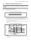
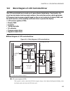
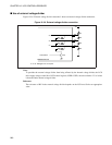
12.2 Block Diagram of LCD Controller/Driver
The LCD controller/driver is made up of seven blocks listed below. Functionally, the
circuit can be broken into two major sections: the controller section, which generates
LCD segment and common signals based on the current contents of display RAM, and
the driver section, which develops sufficient drive to operate the display.
• LCD control register (LCDR)
• Display RAM
• Prescaler
• Timing controller
• V/I converter
• Common output driver
• Segment output driver
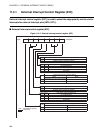
■ Block diagram of LCD controller/driver
Figure 12.2-1 Block diagram of LCD controller/driver
●
LCD control register (LCDR)
This register is used to control the LCD drive supply voltage, select display blanking/non-blanking, select
the display mode, and select the LCD clock cycle.
Internal bus
LCD control register
(LCDR)
Prescaler
Timing
controller
Display RAM
42
x 4-bit
(21 bytes)
F
CH
/ 2
6
Common output driverSegment output driver
V/I converter
4
3
42
Power supply (V1 to V3)
COM0
COM1
COM2
COM3
SEG0
SEG1
SEG2
SEG3
SEG4
SEG37
SEG38
SEG39
SEG40
SEG41
:
:
Controller
Driver
(Timebase timer
output)
FCH: Main clock oscillation frequency