


32
1745D–ATARM–04-Nov-05
AT91M55800A
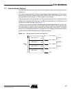
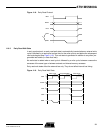
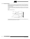
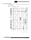
11.7 Write Data Hold Time
During write cycles in both protocols, output data becomes valid after the falling edge of the
NWE signal and remains valid after the rising edge of NWE, as illustrated in the figure below.
The external NWE waveform (on the NWE pin) is used to control the output data timing to
guarantee this operation.
It is therefore necessary to avoid excessive loading of the NWE pins, which could delay the
write signal too long and cause a contention with a subsequent read cycle in standard
protocol.
Figure 11-10. Data Hold Time
In early read protocol the data can remain valid longer than in standard read protocol due to
the additional wait cycle which follows a write access.
ADDR
NWE
Data output
MCK