


116
1745D–ATARM–04-Nov-05
AT91M55800A
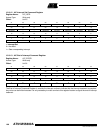
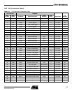
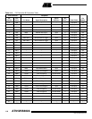
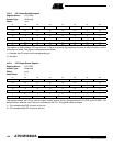
Note: 1. The OFF value is the default level seen on the peripheral input when the PIO line is enabled.
Table 16-2. PIO Controller B Connection Table
PIO Controller Peripheral
Reset State
Pin
Number
Bit
Number
Port
Name Port Name Signal Description
Signal
Direction
OFF
Value
(1)
0 PB0 – – – – PIO Input 139
1 PB1 – – – – PIO Input 140
2 PB2 – – – – PIO Input 141
3 PB3 IRQ4 External Interrupt 4 Input 0 PIO Input 142
4 PB4 IRQ5 External Interrupt 5 Input 0 PIO Input 143
5 PB5 – – – 0 PIO Input 144
6 PB6 AD0TRIG ADC0 External Trigger Input 0 PIO Input 145
7 PB7 AD1TRIG ADC1 External Trigger Input 0 PIO Input 146
8 PB8 – – – – PIO Input 149
9 PB9 – – – – PIO Input 150
10 PB10 – – – – PIO Input 151
11 PB11 – – – – PIO Input 152
12 PB12 – – – – PIO Input 153
13 PB13 – – – – PIO Input 154
14 PB14 – – – – PIO Input 155
15 PB15 – – – – PIO Input 156
16 PB16 – – – – PIO Input 157
17 PB17 – – – – PIO Input 158
18 PB18 BMS Boot Mode Select Input 0 PIO Input 163
19 PB19 TCLK0 Timer 0 Clock signal Input 0 PIO Input 55
20 PB20 TIOA0 Timer 0 Signal A Bi-directional 0 PIO Input 56
21 PB21 TIOB0 Timer 0 Signal B Bi-directional 0 PIO Input 57
22 PB22 TCLK1 Timer 1 Clock signal Input 0 PIO Input 58
23 PB23 TIOA1 Timer 1 Signal A Bi-directional 0 PIO Input 61
24 PB24 TIOB1 Timer 1 Signal B Bi-directional 0 PIO Input 62
25 PB25 TCLK2 Timer 2 Clock signal Input 0 PIO Input 63
26 PB26 TIOA2 Timer 2 Signal A Bi-directional 0 PIO Input 64
27 PB27 TIOB2 Timer 2 Signal B Bi-directional 0 PIO Input 65
28 – – – – – – –
29 – – – – – – –
30 – – – – – – –
31 – – – – – – –