


208
1745D–ATARM–04-Nov-05
AT91M55800A
21.0.1 Analog-to-digital Conversion
The ADC has an internal sample-and-hold circuit that holds the sampled analog value during a
complete conversion.
The reference voltage pin ADVREF allows the analog input conversion range to be set
between 0 and ADVREF. Analog inputs between these voltages convert to values based on a
linear conversion.
The ADC uses the ADC Clock to perform the conversion. To convert a single analog value to
a 10-bit digital data requires 11 ADC clock cycles. The ADC Clock frequency is selected in the
PRESCAL field of the Mode Register (ADC_MR).
21.0.2 Conversion Results
When a conversion is complete, the resulting 10-bit digital value is stored in the Convert Data
Register (ADC_CDR) of the selected channel, and the corresponding EOC flag in the Status
Register (ADC_SR) is set. This bit can provide an interrupt signal and is automatically cleared
when the corresponding Convert Data Register (ADC_CDR) is read.
If the ADC_CDR is not read before further incoming data is converted, the corresponding
Overrun Error (OVRE) flag is set in the Status Register (ADC_SR).
The ADC offers an 8-bit or 10-bit operating mode. By default after a reset, the ADC operates in
10-bit mode. If the bit RES in ADC_MR is set, the 8-bit mode is selected.
When operating in 10-bit mode, the field DATA in ADC_CDR is fully significant.
When operating in 8-bit mode, only the 8 lowest bits of DATA are significant and the 2 highest
bits read 0.
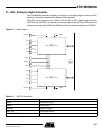
21.0.3 Conversion Triggers
Conversions of the active analog channels are started with a software or a hardware trigger.
The software trigger is provided by writing the bit START in the Control Register (ADC_CR).
The hardware trigger can be one of the TIOA outputs of the Timer Counter channels, or the
external trigger input of the ADC (AD0TRIG for the ADC0 or AD1TRIG for ADC1). The hard-
ware trigger is selected with the field TRGSEL in the Mode Register (ADC_MR). The selected
hardware trigger is enabled with the bit TRGEN in the Mode Register (ADC_MR).
If a hardware trigger is selected, the start of a conversion is detected at each rising edge of the
selected signal. If one of the TIOA outputs is selected, the corresponding Timer Counter chan-
nel must be programmed in Waveform Mode.
Only one start command is necessary to initiate a conversion sequence on all the channels.
The ADC hardware logic automatically performs the conversions on the active channels, then
waits for a new request. The Channel Enable (ADC_CHER) and Channel Disable
(ADC_CHDR) Registers enable the analog channels to be enabled or disabled independently.
21.0.4 Sleep Mode
The AT91 ADC Sleep Mode maximizes power saving by deactivating the ADC when it is not
being used for conversions. Sleep Mode is selected by setting the bit SLEEP in the Mode Reg-
ister ADC_MR.
When a start conversion request occurs, the ADC is automatically activated. As the analog cell
requires a start-up time, the logic waits during this time and starts the conversion sequence on