


186
1745D–ATARM–04-Nov-05
AT91M55800A
Notes: 1. After a hardware reset, the SPI clock is disabled by default. The user must configure the Power Management Controller
before any access to the User Interface of the SPI.
2. After a hardware reset, the SPI pins are deselected by default (see Section 16. ”PIO: Parallel I/O Controller” on page 112).
The user must configure the PIO Controller to enable the corresponding pins for their SPI function. NPCS0/NSS must be
configured as open drain in the Parallel I/O Controller for multi-master operation.
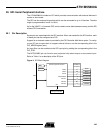
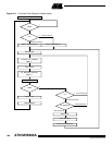
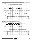
20.2 Master Mode
In Master Mode, the SPI controls data transfers to and from the slave(s) connected to the SPI
bus. The SPI drives the chip select(s) to the slave(s) and the serial clock (SPCK). After
enabling the SPI, a data transfer begins when the ARM core writes to the SP_TDR (Transmit
Data Register).
Transmit and Receive buffers maintain the data flow at a constant rate with a reduced require-
ment for high priority interrupt servicing. When new data is available in the SP_TDR (Transmit
Data Register) the SPI continues to transfer data. If the SP_RDR (Receive Data Register) has
not been read before new data is received, the Overrun Error (OVRES) flag is set.
The delay between the activation of the chip select and the start of the data transfer (DLYBS)
as well as the delay between each data transfer (DLYBCT) can be programmed for each of
the four external chip selects. All data transfer characteristics including the two timing values
are programmed in registers SP_CSR0 to SP_CSR3 (Chip Select Registers). See Table 20-1.
In master mode the peripheral selection can be defined in two different ways:
• Fixed Peripheral Select: SPI exchanges data with only one peripheral
• Variable Peripheral Select: Data can be exchanged with more than one peripheral
Figures 20-1 and 20-2 show the operation of the SPI in Master Mode. For details concerning
the flag and control bits in these diagrams, see the tables in the Programmer’s Model, starting
on page 193.
20.2.1 Fixed Peripheral Select
This mode is ideal for transferring memory blocks without the extra overhead in the transmit
data register to determine the peripheral.
Fixed Peripheral Select is activated by setting bit PS to zero in SP_MR (Mode Register). The
peripheral is defined by the PCS field, also in SP_MR.
This option is only available when the SPI is programmed in master mode.
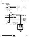
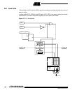
Table 1. SPI Pins
Pin Name Mnemonic Mode Function
Master In Slave Out MISO
Master
Slave
Serial data input to SPI
Serial data output from SPI
Master Out Slave In MOSI
Master
Slave
Serial data output from SPI
Serial data input to SPI
Serial Clock SPCK
Master
Slave
Clock output from SPI
Clock input to SPI
Peripheral Chip Selects NPCS[3:1] Master Select peripherals
Peripheral Chip Select/
Slave Select
NPCS0/
NSS
Master
Master
Slave
Output: Selects peripheral
Input: low causes mode fault
Input: chip select for SPI