


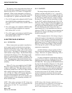

CIRCUIT DESCRIPTION
6-26
March 1999
Part No. 001-2009-600
6.7 800W POWER SUPPLY
WARNING
This power supply contains voltage potentials greater
than 400V. Considering the dangerous voltages and
the complexity of the switch-mode power supply, it is
strongly recommended the power supply be returned
to E.F. Johnson for repair (see Section 1.8).
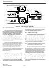
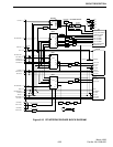
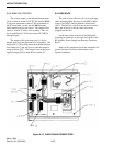
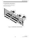
6.7.1 FILTER BOARD
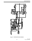
AC power is brought into the power supply
through the IEC connector in the front of the power
supply (see Figure 2-2). This connector is attached to
the EMI filter assembly, Part No. 023-2000-820. The
filter contains common mode and differential mode
filtering such that the supply complies with FCC
Class-A regulations. In addition to the filter compo-
nents (C1, C2, L1, C3, C4, L2, C5) R1 is used to dis-
charge the filter capacitors when AC is removed.
Metal-oxide varistors (RV001/RV002) are placed
across the line on the input and output of the EMI filter
that clamp transients on the AC line to prevent damage
to the power supply. The AC power is fused with
F001 after the connector and before the filter. Replace
fuse with a 15A/250V (314015) fuse.
At the output of the filter board is a bridge recti-
fier. The rectifier is heat sunk to the filter bracket
through a Grafoil thermal interface pad. Filtered AC
power is connected to the main board via wires W001
and W003. Filter and rectified current is brought to
the main board via wires W004 and W005. The safety
ground is connected from the filter board to a stud in
the chassis through W002.
6.7.2 POWER FACTOR CORRECTION
The power factor switching frequency is set at
87.5 kHz, ±5 kHz. The average current mode boost
converter is comprised of L107, Q101, CR145, C110,
C111. Half of U102 is used for power factor correc-
tion. RT101/RT102 are negative temperature coeffi-
cient thermistors that limit the in-rush current to C110/
C111. The resistor network connected to CR104
charges up C106/C107 to +18Voff the line. This pro-
vides the bias voltage required to start the controller
IC U102. Once the IC turns on current is being
switched on L107. A small tap winding on L107 pro-
vides sustaining current to the U102. When AC is first
connected it could take several seconds for C106/C107
to charge to +14V before the unit starts.
U102 samples the input voltage through R105/
R106/R107; the input current through T103/T104/
CR146/CR108/R113/R114; and the output voltage
through the divider at R127. U102 modulates the duty
cycle to MOSFET Q101 such that the input current is
shaped like and in phase with the input voltage. The
controller has two feedback loops; a voltage loop to
keep the 400V constant and a current loop to keep
input current correct. Compensation for the current
error amp is C120/R141/C121 on U102, pin 1. Com-
pensation for the voltage error amp is provided by
C127/C142/C126 on U102, pin 16. U102, pin 4 and
associated circuitry automatically adjust the Power
Factor Correction (PFC) for input voltage (100-240V
AC), line frequency (50-60 Hz) and load on the power
factor.
NOTE: The output voltage of the power factor section
is at 400V DC. This voltage is bled off slowly. After
turning off, it can take more than 5 minutes to dis-
charge.
6.7.3 MAIN PULSE WIDTH MODULATOR
The +26.5V output is created from a two-transis-
tor forward converter Q116/Q118. It uses the 400V
output of the power factor correction on C110/C111
for an input voltage. The same controller IC (U102)
drives the +26.5V stage. This stage runs at exactly
twice the power factor correction frequency and uses
trailing edge modulation. The pulse width modulator
uses the PFC supplied current for modulation scheme
that reduces ripple current in C110/C111.
The output of the IC, U102, pin 11 is fed to a
level shifting gate drive network comprised of C139,
C140, T106, C136, C197, C137 and C228. Each
MOSFET (Q116, Q118) of the two-transistor forward
converter has a gate protection zener diode CR117,
CR120 respectively. In addition, each power MOS-
FET has a gate turnoff network.