


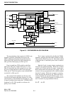

CIRCUIT DESCRIPTION
6-12
March 1999
Part No. 001-2009-600
RF bypass is provided by C416, C418 and C419. The
output of Q403/Q404 is coupled to U403, pin 20 by
C417.
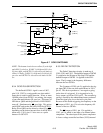
6.2.10 BUFFER AMPLIFIER
A cascode amplifier formed by Q406 and Q407
provides amplification and also isolation between the
VCO and Synthesizer U403. A cascode amplifier is
used because it provides high gain, high isolation and
consumes only a small amount of power. The input
signal to this amplifier is coupled from VCO A007,
pin 6 by C433. C433 also provides DC blocking. Bias
for the amplifier is provided by R450, R451, R453,
R454 and R455. L403 is an RF choke. RF bypass is
provided by C430, C431 and C479. The output of
Q406/Q407 is coupled to U403, pin 11 by a non-polar-
ized capacitor formed by C429/C499.
6.2.11 LOCK DETECT
When the synthesizer is locked on frequency, the
Lock Detect output on U403, pin 2 is a high voltage
with narrow negative-going pulses. When the synthe-
sizer is unlocked, the negative-going pulses are much
wider, the width may vary at a rate determined by the
frequency difference of fV and fR.
The locked or unlocked condition of the synthe-
sizer is filtered by R440/C423 and applied to J401, pin
16, then sent to the RF Interface on J102, pin 16 for
detection.
6.2.12 BUFFER AMPLIFIER
A cascode amplifier formed by Q410/Q411 pro-
vides amplification and also isolation between the
VCO and exciter RF stages. A cascode amplifier is
used because it provides high gain, high isolation and
consumes only a small amount of power. The input
signal to this amplifier is coupled from VCO A007,
pin 4 by C441. C441 also provides DC blocking. Bias
for the amplifier is provided by R464, R465, R466,
R467 and R468. L406 is an RF choke and R463 low-
ers the Q of the coil. RF bypass is provided by C434,
C442, C445, C443, C444 and C480. The output of
Q410/Q411 is matched to the Exciter RF stages by
C446, R450 and two sections of microstrip.
6.2.13 RF AMPLIFIERS
RF amplifier Q412 is biased by CR402, R469,
R470 and R472. C448 provides RF bypass from the
DC line and R471/R472 provide supply voltage isola-
tion. A section of microstrip on the collector acts as
an RF choke to the supply line. Q412 is matched to
Q413 by C449, C451 and two sections of microstrip.
RF amplifier/buffer Q413 is similar in design to
Q412. The collector voltage of Q413 is switched by
Q405. The Logic Push-To-Talk (LPTT) on J401, pin
11 turns on Q405 and conducts the 15V supply to the
collector of Q405 and to Q413. The output of Q413 is
matched to 50 ohms by two sections of microstrip and
C465 that also provides DC blocking. A 3 dB attenua-
tor follows amplifier Q413. The RF output of the
Exciter is on coaxial connector J402 to the Power
Amplifier.
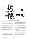
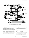
6.3 OCXO DRAWER
6.3.1 INTRODUCTION
The OCXO (Oven Controlled Crystal Oscillator)
drawer produces the 1.25 MHz reference signal input
for the high stability synthesizer loops of both the
Receiver and Exciter. One OCXO drawer alone can
drive eight repeaters. More repeaters can be driven
with the use of external rack mounted 8-Way split-
ters. The signal level at each of the eight outputs is
high enough to allow splitting the signal through an
additional 8-Way splitter to drive additional repeaters.
The OCXOs generate a 10 MHz signal. The fre-
quency stability of these oscillators is better than
0.1 PPM from -40°C to +70°C (-40°F to +158°F).
One half hour after a cold start (at room temperature),
the oscillators will be within 1E-8 of their stabilized
frequency. Two OCXOs are used for redundancy. The
drawer can be configured so that either oscillator is
main and the remaining oscillator will be standby. If
the main oscillator has an output failure, the drawer
will automatically switch to the standby oscillator to
drive the outputs. The oscillators can be switched
between main and standby remotely. The drawer will
not allow remote switching of oscillators if either
oscillator has an output failure.