


CIRCUIT DESCRIPTION
6-14
March 1999
Part No. 001-2009-600
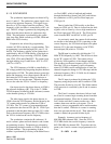
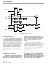
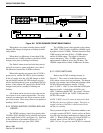
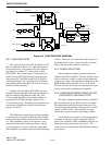
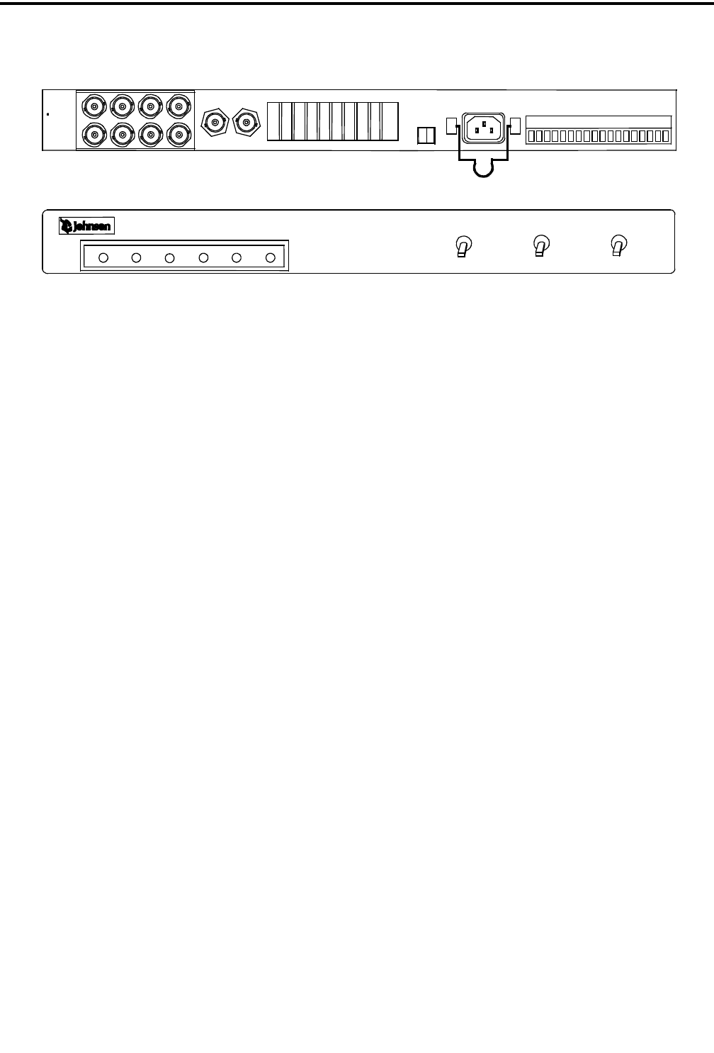
Figure 6-6 OCXO DRAWER FRONT/REAR PANELS
115V
TM
FRONT PANEL
BACK PANEL
IN
OUT
10 MHz
1.25 MHz
OUTPUTS
OCXO2
DELTA F
OUTPUT
AC DCOCXO1
OCXO 2
INTERRUPT
OCXO 1
INTERRUPTINTERRUPT
DC BACKUP
FOR PROPER STABILIZATION
ALLOW 30 MINUTES WARM UP
1615 17185 6 7 8 91011121314
1
234
When there is no output from the drawer, the RF
Output LED changes from green to flashing red indi-
cating failure.
When there is a difference of more than 10 Hz
between the two 10 MHz oscillators, the Delta F LED
changes from green to flashing red (failure).
The Delta F alarm circuit has built in hysteresis
and will not return to green until there is less than 5
Hz difference between the 10 MHz oscillators.
When both supplies are present, the AC LED is
green (active), and the DC LED is yellow (standby).
If the AC supply fails, the AC LED changes to flash-
ing red (failure) and the DC LED changes to green
(active) indicating that it is now powering the OCXO
drawer. If the external DC supply fails, the DC LED
changes from yellow (standby) to flashing red
(failure).
All of these alarms are tied to relays that can be
set to open or close contacts upon alarms. The relay
contacts are connected to the 18-pin connector at the
rear of the drawer. These relay contacts are capable of
handling 1A DC current.
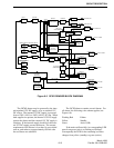
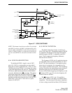
6.3.2 OCXOS, BUFFERS, DIVIDER AND LINE
DRIVER
The OCXOs produce a signal level greater than
1V RMS. Q901 and Q902 serve as buffers and square
up the signal from 0 to 5V (see Figure 6-5). Selection
of the oscillators as described in Section 6.3.1 is
accomplished by the logic gates U901-U904.
The 10 MHz signal is then applied to the counter
chip U905. U905 is used to divide the 10 MHz signal
by eight to create 1.25 MHz. The dual line driver chip
U906 is used to drive the 8-Way 1.25 MHz outputs
and the 10 MHz output. The signal is filtered to
remove harmonics. The 1.25 MHz outputs have
approximately 0 dBm of power into 50 ohms. The
10 MHz output delivers about 10 dBm into 50 ohms.
6.3.3 OCXO SWITCHING
Refer to the OCXO switching circuitry in
Figure 6-7. The circuit is broken down into three
levels where various tasks are performed. The bottom
section is for remote control input and selecting which
OCXO LED should indicate standby. U902A,
pins 1-2 (OSC 1 - OSC 2) come from the OCXO pulse
detector circuits. A logic high on U902A, pin 1
(OSC 1) indicates that OCXO 1 has output. Likewise,
a logic high on U902A, pin 2 (OSC 2) indicates that
OCXO 2 has output.
NOTE: U902C, pin 8 (S) cannot be high unless both
OCXO pulse detectors indicate output. Therefore, no
remote switching of OCXOs is allowed unless both
OCXOs are running.
The top section of Figure 6-7 determines whether or not
a switch is made to OCXO 2. In this section, an Exclu-
sive OR logic decision is made between inputs (S) and
(OSC 1). When U902B, pin 6 (X) is high, OCXO 1 is
selected, when it is low, OCXO 2 is selected. If
(OSC 1) is low, (X) goes low and OCXO 2 is selected.