


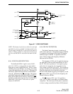
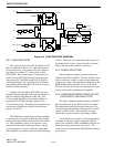
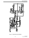

CIRCUIT DESCRIPTION
6-23
March 1999
Part No. 001-2009-600
Pin 10 GROUND
Pin 11 LPTT
The Logic Push-To-Talk (LPTT) is an open col-
lector from the Controller. It has a sink capability of
20 mA nominal and a voltage rating of 18V maxi-
mum. The transmitter should produce power when
this pin is a logic low.
Pin 12 SYN CS EX
Pin 12 is the Exciter main synthesizer chip select.
It allows data input to the specific synthesizer chip
when the line is pulled to a logic low.
Pin 13 TX MOD
The audio from the MAC in the Controller pro-
cesses a number of inputs to the station per the TIA
specifications to produce the signal on this pin. This
signal goes through the RFIB and then to the Exciter.
A 707 mV RMS (2V P-P) sine wave at 1 kHz provides
60% of system deviation in the transmitter. The DC
voltage on the line is 3.5V ±0.1V. The source imped-
ance should be low (output of an op-amp or analog
switch < 200 ohms) and the input impedance will not
be less than 10k ohms.
Pins 14-15 GROUND
These pins carry ground current between the
RFIB and the Exciter board.
Pin 16 SYN LK EX
Pin 16 is the Exciter main synthesizer lock detec-
tor output. The synthesizer is locked with a TTL logic
high state.
Pin 17 HS LK EX
Pin 17 is the high stability synthesizer lock detec-
tor output for the 900 MHz Exciter. The synthesizer is
locked with a TTL logic high state.
Pin 18 HS CS EX
This input goes low to enable the loading of data
into the exciter high stability synthesizer chip U401.
Pin 19 RF CLK
The clock controls the Exciter synthesizer when
loading. The input source in the Controller is TTL
with the speed determined by the synthesizer chip.
There could be as many as four synthesizers and a
shift register.
Pin 20 RF DATA
Pin 20 is a data pin from the Controller which has
the dual role of loading the synthesizer chip and
adjusting the power control D/A lines for proper out-
put power. The data has TTL levels. Up to four syn-
thesizer chips and a shift register could be connected
to this pin.
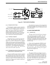
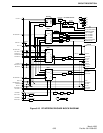
6.6.6 RECEIVER CONNECTOR (J103)
The connector from the Receiver (J201) to the
RF Interface board (J103) links the Receiver to the
MPC in the Controller Backplane.
Pin 1 VCC1
Pin 1 is fused +15V ±1% with a nominal current
of 1A provides current from the RFIB to the Receiver.
Pins 2-6 UNUSED
Pin 7 RSSI
This pin is the Receive Signal Strength Indicator
(RSSI) to the Controller. The RSSI is used for tune-
up of the Receiver front-end during test mode. The
dynamic range is 60 dB. Output from an op-amp with
the voltage going from 0.5V to 4.5V. The level has an
adjustment in the Receiver.
Pin 8 UNUSED
Pin 9 RX WBAND
The receive wide band audio is from the demodu-
lator and goes to the Main Audio Card (MAC) in the
Controller card cage. The typical amplitude is 387
mV RMS (-6 dBm) and 2V DC with Standard TIA
Test Modulation into the Receiver. Little wave shap-
ing is done on the Receiver board other than a 31 kHz
RC LPF which strips off the 450 kHz IF. Buffering is
done with an op-amp which can drive a 10k ohm load.