


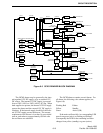

CIRCUIT DESCRIPTION
6-20
March 1999
Part No. 001-2009-600
Pin 13 RF MUX1 INH
The Multiplexer-1 Inhibit (U105, pin 6) is a
CMOS input from the Controller that inhibits (dis-
ables) the output from the RF 1 Multiplexer with a
logic high.
Pin 14 V REF EX
This is the 3.5V reference to the Exciter TCXO.
3.5V from the Exciter is passed from J102, pin 9 to
this pin and the backplane. The voltage then passes
through the MAC and back to the backplane to J101,
pin 22 with the TX MOD. These are connected to
J102, pin 13 back to the Exciter.
Pins 15-18 UNUSED
Pin 19 RF MUX3 INH
The Multiplexer-3 Inhibit (U104, pin 6) is a
CMOS input from the Controller that inhibits (dis-
ables) the output from the RF 3 Multiplexer with a
logic high.
Pin 20 LPTT
The Logic Push-To-Talk is an open collector
from the Controller. It has a sink capability of
20 mA and a maximum voltage rating of 18V. The
transmitter should produce power when this pin is a
logic low.
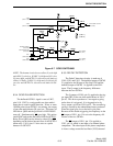
Pin 21 SYN CS EX
This input goes low to enable the loading of data
into the exciter main synthesizer chip U403.
Pin 22 TX MOD
The audio from the MAC in the Controller pro-
cesses a number of inputs to the station to produce the
signals on this pin. This signal goes through the RFIB
and then to the Exciter. A 707 mV RMS sine wave
(2V P-P) at 1 kHz produces 60% of system deviation
in the transmitter. The source impedance is low and
the input impedance is less than 10k ohms.
Pin 23 GROUND
Pin 23 carries ground current between the RFIB
and CBP board.
Pin 24 UNUSED
Pin 25 LOGIC CONTROL TO FANS
Pin 25 is in parallel with the temperature sensor.
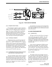
Pin 26 RF DATA B
The Data B (U105, pin 10) is the middle signifi-
cant bit in the three multiplex chips located on the
RFIB. This pin is a CMOS input from the Controller
requiring a logic high for activation.
Pin 27 A D LEVEL
20 lines (of the possible 24) of RF functions sam-
pled are multiplexed to the Controller through this pin
using three multiplex chips.
• RF Forward Power Sense
• RF Power Sense Device 1
• RF Power Sense Device 2
• RF Power Sense Device 3
• RF Power Sense Device 4
• RF Reflected Power Sense
• PA Temperature
• Transmit Audio Modulation
• High Stability Exciter Lock Detector
• Exciter Lock Detector
• Receiver Detector Audio
• Receive Signal Strength Indicator
• Receiver Injection Level
• High Stability Receive Lock Detector
• Receiver Lock Detector
• Fan Current 1
• Fan Current 2
• Fan 1 On Sense
• Power Supply Temp
• Battery Voltage
Pin 28 RF DATA
A data pin with TTL levels from the Controller
which has the dual role of loading the synthesizer
chips and adjusting the power control D/A lines for
proper output power. Up to four synthesizer chips and
a shift-register could be connected to this pin.
Pin 29 SYN CS RX
This input goes low to enable the loading of data
into the receiver main synthesizer chip U209.