


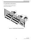

CIRCUIT DESCRIPTION
6-29
March 1999
Part No. 001-2009-600
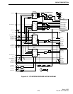
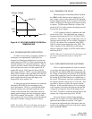
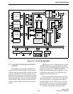
6.7.6 +15V CONVERTER
The input voltage to this "Buck" DC/DC con-
verter is the main +26.5V output fused through F102.
The bias voltage for the controller IC U112, pin 15 is
provided by a +15V regulator U111. The basic buck
converter consists of MOSFET Q125, Schottky diode
CR126 and storage inductor L102. C165, C166,
C167, L103, C169 and C170 filter the output voltage
and attenuate the ripple at the switching frequency
(160 kHz). The capacitors are an integral part of the
feedback loop. The duty cycle is approximately 60%.
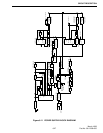
The +15V buck converter is peak current mode
controlled. T108 samples the inductor current while
MOSFET Q125 is on. The sampled current is trans-
lated to a voltage via CR127, R209 and R210.
Because the MOSFET is a high-side switch, a
charge pump is required to get the gate voltage above
the input voltage. The charge pump operates as fol-
lows. When the output from IC U112, pin 14 is low,
capacitor C162 is charged through CR124, R198,
R199, R200 and Q122/Q123 are off. When U112, pin
14 goes high, the capacitor stays charged and CR124
is reverse biased. Q122/Q123 are turned on forward
biasing CR125 and applying a gate-to-source voltage
of approximately +12V. During this time Q124 is off.
When U112, pin 14 goes low, Q124 turns on and rap-
idly discharges the gate capacitance.
Resistors R231/R208 coupled with C164 provide
snubbing for Schottky diode CR126.
Because the +15V converter operates at greater
than 50% duty cycle, slope compensation is required.
Capacitor C176 is the time capacitor for this converter
and R223 is the resistor that sets the charge current. A
sawtooth wave is present on the high side of C176 that
is buffered by Q127/Q128. The resistor divider net-
work of R315, R227, R229 and R232 provide the cor-
rect amount of compensation for stable operation and
current limiting.
The output voltage is sampled by R215, R216 and
R217 and sent to the inverting side of the error ampli-
fier internal to the controller IC on U112, pin 1. Volt-
age loop compensation is set by C174, C175 and
R221.
Sync pulse is added into the low side of C176 via
C172 and R225. The free running frequency of the
15V converter (approximately 145 kHz) is set about
10% lower than the 26.5V converter. This longer duty
cycle allows the sync circuit to synchronize the con-
verter.
Over voltage is sensed using U116 as a reference
and amplifier, CR129 acts as a crowbar on the output.
Once the crowbar is turned on, opto-isolator U119 is
activated to shutdown the power supply. The enable
line must be toggled or AC voltage removed for 10
seconds to reset the power supply.
6.7.7 +5V CONVERTER
Operation of the +5V "Buck" DC/DC converter is
the same as the +15V, except slop compensation is not
required. Some values are different to get the 5.2V
DC and current limit to 6A. The duty cycle is approxi-
mately 20%.
6.7.8 -5V CONVERTER
The -5V "Buck-Boost" converter scales and
inverts the voltage. This converter is free running at
approximately 75 kHz. The output switch and control-
ler are built into the 5-leg TO-220 IC U114. L105 is
the storage inductor. C204, R270 and R271 close the
voltage feedback loop and are set for optimum stable
transient response. C208/C209 reduce output ripple.
Under-voltage protection is required on this stage and
works the same as the over-voltage protection of the
+15V and +5V buck converters, but has opposite
polarity.
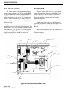
6.7.9 POWER SUPPLY REPAIR AND ALIGN-
MENT
If a power supply fails it is typically a Power
MOSFET or Power Diode. In some cases the MOS-
FET gate may short and cause some of the driver cir-
cuits to be damaged. When replacing heat sunk com-
ponents it is advisable to replace the sil-pad thermal
interface material at the same time. The mounting
hardware must be replaced exactly as built in the fac-
tory. The mounting screws for the power semiconduc-
tors MUST BE torqued to 4-5 in/lbs. Under torque
and over torque can shorten the life of the semicon-
ductor.