CIRCUIT DESCRIPTION
6-7
March 1999
Part No. 001-2009-600
NOTE: Section 8.2.5 describes how the N and A
counter numbers are calculated for other channels.
To determine the overall divide number of the
prescaler and N counter, the number of VCO output
pulses required to produce one N counter output pulse
can be counted. In this example, the prescaler divides
by 65 for 65 x 60 or 3,900 input pulses. It then
divides by 64 for 64 x (1056 - 60) or 63,744 input
pulses.
The overall divide number K is therefore
(3,900 + 63,744) or 67,644. The VCO frequency of
845.5500 MHz divided by 67,644 equals 12.5 kHz
which is the fR input to the phase detector. The over-
all divide number K can also be determined by the fol-
lowing formula: K = 64N + A
Where,
N = N counter divide number and
A = A counter divide number.
6.1.16 BUFFER AMPLIFIER
A cascode amplifier formed by Q210 and Q211
provides amplification and also isolation between the
TCXO and Synthesizer U209. A cascode amplifier is
used because it provides high reverse isolation. The
input signal to this amplifier is from TCXO Y201.
C254 provides DC blocking. Bias for the amplifier is
provided by R312, R248, R249, R251 and R250.
L218 is an RF choke. RF bypass is provided by C251,
C252 and C253. The output of Q210/Q211 is coupled
to U209 by C307.
6.1.17 LOCK DETECT
When the synthesizer is locked on frequency, the
Lock Detect on U209, pin 2 is a high voltage with
very narrow negative-going pulses. Then when the
synthesizer is unlocked, these pulses become much
wider, the width may vary at a rate determined by the
frequency difference of fV and fR.
The lock detect pulses are filtered by R270/C325
and applied to J201, pin 14 and the RF Interface on
J103, pin 14 for detection and sampling in the IAC.
6.1.18 BUFFER AMPLIFIER
A cascode amplifier formed by Q214 and Q215
provides amplification and also isolation between the
VCO and Receiver RF stages. A cascode amplifier is
used because it provides high reverse isolation. The
input signal to this amplifier is coupled from VCO
A006 by C268. C268 also provides DC blocking.
Bias for the amplifier is provided by R294, R311,
R290, R291 and R292. L222 is an RF choke and
R293 lowers the Q of the coil. RF bypass is provided
by C274, C356, C310, C272, C273 and C335. The
output of Q214/Q215 is matched to the Receiver RF
stages by C275, C276 and two sections of microstrip.
6.1.19 RF AMPLIFIERS
U210 provides the +12V source for these ampli-
fiers. RF amplifier Q216 is biased by R296 and R295.
C278 provides RF bypass from the DC line and R297
provides supply voltage isolation. A section of
microstrip on the collector acts as an RF inductor.
Q216 is matched to Q217 by C277, C263, C288 and
two sections of microstrip.
RF amplifier/buffer Q217 is similar in design to
Q216. The output of Q217 is matched to the 3 dB
attenuator made up of R285/R286/R287 by two
sections of microstrip and C280 provides DC block-
ing. L223/L224 are tuned to the receive frequency
minus 52.95 MHz and passed to Mixer U201. This
injection frequency is also coupled through C284 to
U204A. CR201, R255, R254 provide DC input to
U204A, pin 3. The output of U204A, pin 1 is con-
nected to J201, pin 13 for a receive injection test point
and connected to the RF Interface Board on J103,
pin 13.
6.2 EXCITER
6.2.1 VCO (A007)
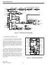
The VCO (Voltage-Controlled Oscillator) is
formed by Q802, associated circuitry and a resonator
consisting of L404 in the Exciter. The screw in L404
tunes the tank circuit to the desired frequency range.
The VCO oscillates in a frequency range from
935-940 MHz. Biasing of Q802 is provided by R805,
R806 and R807. An AC voltage divider formed by
C812 and C813 initiates and maintains oscillation.


