


CIRCUIT DESCRIPTION
6-19
March 1999
Part No. 001-2009-600
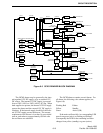
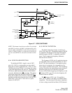
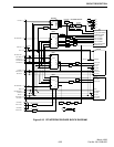
6.6 RF INTERFACE BOARD
The RF Interface Board connects the Receiver,
Exciter and Power Amplifier to the backplane and
power supply (see Figure 6-10).
The input and output connectors for the RF Inter-
face Board are defined as follows.
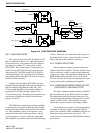
6.6.1 POWER CONNECTOR
The power supply is connected to the RF Inter-
face Board when the RF module is inserted into the
station cabinet (see Figure 10-7). The jack portion of
the connection is on the RF Interface Board, the plug
portion is attached to the repeater cabinet.
P101/P102 +26.5V DC - Supply voltage to PA.
+26.5V ±1%, 12A at 75W and 20A nominal (24A max-
imum) at 160W.
P103 +15V DC - Supply voltage to Exciter, Receiver
and Power Control. 15V ±1%, 5.5A max.
P104/P105 GROUND - Ground return for the RF as-
sembly.
6.6.2 SIGNAL CONNECTOR (J101)
This is the signal interface connector J101 (36
pin) that connects the RF Interface board to the back-
plane connector J2 (34 pin) through cable assembly
A8.
Pin 1 GROUND
Pin 1 carries ground current between the RF
Interface board and Backplane board.
Pin 2 PC STR
Pin 2 is the Power Control Strobe. This is nor-
mally low until after the power control data is shifted
into the power control register. Then the strobe line
goes high and back to low. The clock or data lines
cannot be changed until after the strobe is set.
Pin 3 HS CS EX
Pin 3 is used in the 900 MHz repeater only. A
low enables the high stability synthesizer loop.
Pin 4 GROUND
Pin 4 carries ground current between the RF
Interface board and Backplane board.
Pins 5-6 UNUSED
Pin 7 RX WBAND
The wide band audio is from the receive audio
demodulator U202 and goes to the MAC in the Con-
troller card cage. The typical amplitude is 387 mV
RMS (-6 dBm) and 2V DC with Standard TIA Test
Modulation into the receiver. Little wave shaping is
done on the receiver board other than a 31 kHz RC
LPF which strips off the 450 kHz IF. Buffering is
done with an op-amp.
Pin 8 RF DATA A
Data A (U105, pin 11) is the least significant bit
(LSB) in the 3 multiplex chips located on the RFIB.
This pin is a CMOS input from the Controller requir-
ing a logic high for activation.
Pin 9 RF DATA C
Data C (U105, pin 9) is the most significant bit
(MSB) in the 3 multiplex chips located on the RFIB.
This pin is a CMOS input from the Controller requir-
ing a logic high for activation.
Pin 10 RF MUX2 INH
The Multiplexer-2 Inhibit (U106, pin 6) is a
CMOS input from the Controller that inhibits (dis-
ables) the output from the RF 2 Multiplexer with a
logic high.
Pin 11 RF CLK
The clock will control the synthesizer chips and
power control circuit when loading. This pin is a TTL
input from the Controller.
Pin 12 HS CS RX
This input goes low to enable the loading of data
into the receiver high stability synthesizer chip U205.