


CIRCUIT DESCRIPTION
6-16
March 1999
Part No. 001-2009-600
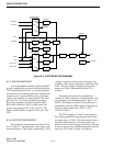
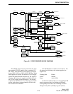
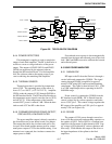
to U913. The output of this phase comparator at
U911, pin 13 is essentially low if the input from the
VCO is higher in frequency than the input from U911,
pin 12. Conversely, this output is essentially high if
the input from the VCO is lower in frequency than the
input from U911, pin 12. Clocking pulses are continu-
ally present on the PCP output of U913, pin 1.
The VCO oscillates at either the high or low end
of its operating range, depending on the logic level
present on the control input of U913, pin 9. If the
control input is high, it oscillates at the high end of its
range. If the control input is low, it oscillates at the
low end of its range. The high frequency is approxi-
mately 20 Hz and the low frequency is approximately
10 Hz. During normal operation, the Q output of the
flip-flop in U910, pin 8 is high and the VCO oscillates
at 20 Hz.
When the frequency difference between OCXOs
exceeds about 10 Hz (1 PPM), the frequency of the
signal from U911, pin 12 exceeds the VCO fre-
quency. Recall that the frequency difference is dou-
bled by U911. The output from the phase comparator
on U913, pin 13 goes high and the Q outputs of flip-
flop U910B change state. This turns on red LED
DS904. The Q output of U910, pin 9 now applies a
logic low to the VCO control input of U913, pin 9 and
the VCO goes to its low frequency limit (10 Hz).
Therefore, the OCXO frequency difference must
decrease to less than 5 Hz for the alarm to be can-
celed. This hysteresis prevents intermittent triggering
when the frequency difference is near the triggering
point.
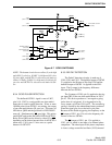
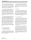
6.4 75W POWER AMPLIFIER
6.4.1 AMPLIFIER/PRE-DRIVER
RF input to the PA from the Exciter is through a
coaxial cable and connector to WO511. C501 couples
the RF to 50 ohm microstrip that connects the input to
U501. U501 is a 6W amplifier/pre- driver operating
in the 935-940 MHz band.
Power control is connected to WO505 from the
RF Interface board (RFIB). RF is filtered from the
control voltage line by various capacitors and induc-
tors to U501, pin 2. This control voltage regulates the
RF output of the amplifier on U501, pin 4 to approxi-
mately 5W.
6.4.2 DRIVER
The output of U501 passes through several sec-
tions of 50 ohm microstrip and matching capacitors to
the emitter of Q501. Driver Q501 is a common- base
amplifier with a normal output of approximately 22W.
Supply voltage is RF bypassed by various capacitors
and microstrip. C525/C526/C536/ C537/C538/C589
match the output of the driver to the input impedance
of the combiner to the final amplifiers.
6.4.3 FINAL AMPLIFIERS
Q502 and Q503 are combined 60W amplifiers.
A 50 ohm microstrip connects the RF to a 70.7 ohm
Wilkinson splitter and then to the emitter of each com-
mon-base amplifier. The 60W outputs on the collec-
tors of the amplifiers are combined using a Wilkinson
combiner. Q502 has a half-wave transmission line on
the input and Q503 has a half-wave on the output.
These transmission lines are used to drive the 60W
amplifiers out of phase. The output of the combiner is
fed from WO513 directly to the forward/reverse
power detect board.
The Wilkinson splitter and combiner provide the
capability to split the drive input and combine the
final outputs while maintaining isolation between the
two final amplifiers. The combiner consists of two
quarter-wave transmission lines and a balancing resis-
tor. During normal operation, signals of relatively
equal phase and amplitude are present on both ends of
the balancing resistor. Therefore, no current flows and
no power is dissipated in the balance resistor. If one
final fails, the other final of the pair continues to
function.