


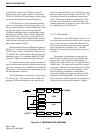
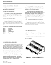
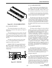
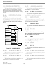


CIRCUIT DESCRIPTION
6-50
March 1999
Part No. 001-2009-600
Pin 9 AC FAIL IN
This input from the AC supply is used by the AC
fail output to indicate that the AC has been interrupted.
Pin 10 SYN CS RX
This is the chip select pin for the main receiver
synthesizer chip. This chip is the same part as used in
the Exciter. A low loads the synthesizer.
Pin 11 UNUSED
Pin 12 RF MUX 1 INH
The Multiplexer-1 Inhibit (U105, pin 6) is a
CMOS input from the Controller that inhibits (dis-
ables) the Multiplexer-1 output with a logic high.
Pin 13 RF MUX 2 INH
The Multiplexer-2 Inhibit (U106, pin 6) is a
CMOS input from the Controller that inhibits (dis-
ables) the Multiplexer-2 output with a logic high.
Pin 14 RF MUX 3 INH
The Multiplexer-3 Inhibit (U104, pin 6) is a
CMOS input from the Controller that inhibits (dis-
ables) the output from the RF 3 Multiplexer with a
logic high.
Pin 15 PC STR
The Power Control Strobe is normally low until
after the power control data is shifted into the power
control register. Then the strobe line goes high and
back to low. The clock or data lines cannot be
changed until after the strobe is set.
Pin 16 HS CS EX
This is the 900 MHz Exciter high stability synthe-
sizer chip select. A low enables loading the high sta-
bility synthesizer loop.
Pins 19-21 UNUSED
Pin 22 BUF RX WBAND
This is buffered Receive Wide Band Audio from
the Receiver audio demodulator through the RF Inter-
face Board. The typical amplitude is 387 mV RMS (-
6 dBm) and 5V DC with Standard TIA Test Modula-
tion into the receiver. This is an output to the rear con-
nector J1.
Pin 23 AC FAIL OUT
This is an indication that the AC power has been
interrupted.
Pin 24 UNUSED
Pin 25 HS CS RX
This is the 900 MHz Receiver high stability syn-
thesizer chip select. A low enables loading the high
stability synthesizer loop.
Pin 26 SYN CS EX
Pin 26 is the main Synthesizer Chip Select in the
Exciter that allows input of data to the specific synthe-
sizer chip when the line is pulled to logic low.
Pin 27 UNUSED
Pin 28 A D LEVEL
20 lines (of the possible 24) of RF functions sam-
pled are multiplexed to the Controller through this pin
using three multiplex chips.
Pin 29 RF DATA A
Data A (U105, pin 11) is the least significant bit
(LSB) in the 3 multiplex chips located on the RFIB.
This pin is a CMOS input from the Controller requir-
ing a logic high for activation.
Pin 30 RF DATA B
Data B (U105, pin 10) is the middle significant
bit in the 3 multiplex chips located on the RFIB. This
pin is a CMOS input from the Controller requiring a
logic high for activation.