


CIRCUIT DESCRIPTION
6-8
March 1999
Part No. 001-2009-600
C803 couples Q802 to resonator L404 in the Exciter.
Resonator L404 provides the shunt inductance of the
tank circuit. The shunt capacitance of the tank circuit
is made primarily of C804 in series with CR802. RF
choke L805 completes the DC bias path to ground.
The VCO frequency is controlled in part by DC
voltage across varactor diode CR802. As voltage
across a reverse-biased varactor diode increases, its
capacitance decreases. Therefore, VCO frequency
increases as the control voltage increases. The control
line is RF isolated from tank circuit by choke L804.
The amount of frequency change produced by CR802
is controlled by series capacitor C804.
The frequency is modulated in a similar manner.
The transmit audio/data signal is applied across varac-
tor diode CR801 to vary the VCO frequency at an
audio rate. C802 in series with CR801 determine the
amount of modulation produced by the audio signal.
6.2.2 EXCITER VCO AND TCXO FREQUENCY
MODULATION
Both the VCO and TCXO are modulated in order
to achieve the required frequency response. If only
the VCO was modulated, the phase detector in U403
would sense the frequency change and increase or
decrease the VCO control voltage to counteract the
change (at the lower audio frequencies inside the
closed loop bandwidth of the synthesizer). If only the
TCXO frequency was modulated, the VCO would not
track the higher audio frequencies (those beyond the
closed loop bandwidth of the synthesizer). However,
by modulating both the VCO and TCXO a flat audio
response is achieved. Potentiometers R425 and R446
balance the modulating signals.
There are two 3.5V sources on the Exciter board;
one is a reference for the modulation amplifier to the
VCO, the other is for the modulation amplifier to the
TCXO.
The reference voltage on U402B, pin 5 is sent to
buffer U407B, J401, pin 9 to RFIB connector J102,
pin 9 and out on J101, pin 14 to J2, pin 27 on the
backplane, to the bottom connectors via pin 7 and
finally to the MAC on P100, pin 7.
With reference to the ground on the Exciter, the
3.5V reference stability is maintained by U126B/C/D
on the MAC. The 3.5V DC passes through summing
amplifier U129B and transmit modulation gate U118D
to P100, pin 29 (Tx MOD). P100, pin 29 is connected
to backplane connector J2, pin 8 and RFIB connector
J101, pin 22 to J102, pin 13. The transmit modulation
and 3.5V reference enter the Exciter on J401, pin 13
and is routed to U402B,pin 6. R425 sets the TCXO
modulation level. The modulation signal along with
the 3.5V DC is applied to U402A, pin 2.
6.2.3 ACTIVE FILTER
Q801 functions as a capacitance multiplier to
provide filtering of the 12V supply to Q802. R801
and R802 provide transistor bias, and C809 provides
capacitance that is effectively multiplied by the gain
of Q801. If a noise pulse or other quick voltage
change appears on the collector, base voltage does not
change significantly because of C809. Therefore, the
base current does not change and transistor current
remains constant. R803 decouples the VCO output
from AC ground. L803 is an RF choke and C807/
C808/C810/C811 provide RF bypass.
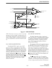
6.2.4 BUFFER
A cascode amplifier formed by Q406/Q407 pro-
vides amplification and isolation between the VCO
and synthesizer. A cascode amplifier is used because
it provides high reverse isolation. The input signal to
this amplifier is tapped from the VCO RF output. DC
blocking and coupling to the VCO is provided by
C441 and to the buffer by C433. Bias for the ampli-
fier is provided by R451, R453, R454 and R455.
Q407 is a common-emitter amplifier and Q406 is a
common-base with C432 providing RF bypass. L403
decouples the output from AC ground and R452 low-
ers the Q of L403. The amplifier is coupled by C429
and C499 to U403, pin 11.
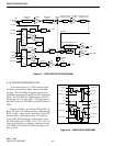
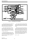
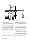
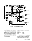
6.2.5 HIGH STABILITY SYNTHESIZER
The High Stability synthesizer inputs/outputs are
shown in Figures 6-3 and 6-4. The synthesizer con-
tains the R (reference), N, and A counters, phase and
lock detectors and counter programming circuitry.
The phase detector output signal of Synthesizer U401,
pin 6 is a 10 kHz pulse waveform from 0 to 5V.