


CIRCUIT DESCRIPTION
6-9
March 1999
Part No. 001-2009-600
This signal is integrated to provide a DC tuning
voltage for the TCXO. The DC tuning voltage pro-
vides the TCXO with the ±0.1 PPM stability of the
OCXO (see Section 6.3).
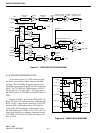
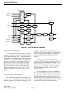
The phase detector output signal is generated by
counters in U401 programmed to divide by a certain
number. This programming is provided through
J401, pins 18, 19 and 20. The frequency stability of
the High Stability synthesizer is established by the
±0.1 PPM stability of the OCXO, stable from -40°C to
+70°C (-40°F to +158°F).
The phase detector in U401 compares the phase
and frequency of two input signals; fR and fV. The
phase detector generates a 0 to 5V signal. The pulse
width of this signal varies depending on the phase dif-
ference between fR and fV. This signal is filtered
(integrated) by C406/C407/C408/R411/R412 to pro-
vide a DC tuning voltage for the TCXO. The voltage
at U402A, pin 1 is set for 3.5V when the high stability
loop is locked. This is done by adjusting the tuning
screw in TCXO Y401.
One input signal is the reference frequency (fR).
This frequency is the 1.25 MHz OCXO frequency
divided by the reference counter to 10 kHz.
The other input signal to the phase detector in
U401 is from the TCXO frequency divided by the "N"
counter and prescaler in U401. The N counter is pro-
grammed through the synthesizer data line on J401,
pin 20. U401 is programmed so the phase detector
input (fV) is identical to the reference frequency (fR).
High Stability synthesizer programming does not
change with channel selection.
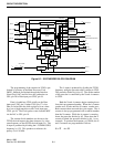
The programming of the counters in U401 is per-
formed by circuitry in the Main Processor Card
(MPC), buffered and latched through the Interface
Alarm Card (IAC) and fed in to the synthesizer on
J401, pin 20 to Data input port U401, pin 19.
Data is loaded into U401 serially on the Data
input port U401, pin 19 when U401, pin 17 is low.
Data is clocked into the shift registers a bit at a time
by a low to high transition on the Clock input port
U401, pin 18. The Clock pulses come from the MPC
via the IAC to J401, pin 19.
The counter divide numbers are chosen so the
TCXO derived input to the phase detector (fV) is
the same frequency as the OCXO derived input (fR).
The fR input is produced by dividing the 1.25 MHz
OCXO frequency by 125 to produce a reference fre-
quency (fR) of 10 kHz.
The fV input is produced by dividing the TCXO
frequency using the prescaler and N counter in U401.
The prescaler divides by 64 or 65. The prescaler
divide number is controlled by the N and A counters
in U401. The N and A counters function as follows:
Both the N and A counters begin counting down
from their programmed number. When the A counter
reaches zero, it halts until the N counter reaches zero.
Both counters then reset and the cycle repeats. The A
counter is always programmed with a smaller number
than the N counter. While the A counter is counting
down, the prescaler divides by 65. Then when the A
counter is halted, the prescaler divides by 64.
Example: To produce the 10 kHz frequency, the
N and A counters are programmed as follows:
N = 27 A = 22
To determine the overall divide number of the
prescaler and N counter, the number of TCXO output
pulses required to produce one N counter output pulse
can be counted. In this example, the prescaler divides
by 65 for 65 x 22 or 1430 input pulses. It then divides
by 64 for 64 x (27 - 22) or 320 input pulses. The over-
all divide number K is therefore (320 + 1430) or 1750.
The TCXO frequency of 17.5000 MHz divided by
1750 equals 10 kHz which is the fR input to the phase
detector. The overall divide number K can also be
determined by the following formula:
K = 64N + A
Where,
N = N counter divide number and
A = A counter divide number.
6.2.6 LOCK DETECT
When the synthesizer is locked on frequency, the
Lock Detect output on U401, pin 2 is a logic high
voltage with narrow negative-going pulses. When the
synthesizer is unlocked, the negative- going pulses are
much wider, the width may vary at a rate determined
by the frequency difference of f
V and fR. The lock
detect pulses of U401 are filtered by R407/C401 and
applied to J401, pin 17, then sent to the RFIB on J102,
pin 17 for detection.