CIRCUIT DESCRIPTION
6-34
March 1999
Part No. 001-2009-600
6.11 MAIN PROCESSOR CARD
6.11.1 INTRODUCTION
The Main Processor Card (MPC) connects to the
computer with repeater software to program the
repeater parameters, sets and reads the alarms, han-
dles communication between repeaters, maintains the
audio gating for the MAC, handles initialization
requests from cards and contains the repeater RF data
for the Receiver, Exciter and CWID.
Control functions for each repeater are per-
formed by the Main Processor in the MPC installed in
each repeater. The MPC contains the main software
and control over the repeater via microprocessor U27
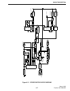
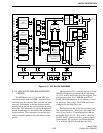
(see Figure 6-23).
Information is exchanged between repeaters via a
High-Speed Data Bus (HSDB) that interconnects all
the MPCs. This control technique is called distribu-
tive processing and it eliminates the need for a sepa-
rate system controller at each site. The HSDB proces-
sor (U13) on the MPC provides these control
functions.
The MPC also contains:
• Flash Memory, RAM, non-volatile EEPROM.
• I/O chip select to allow the addressing of data
latches for Input/Output.
• Read/Write selection to be sent and received on the
Controller Backplane.
• Clock line, data line and chip select line from the
IAC to load the Receiver and Exciter synthesizers.
• Serial communication circuitry and processes for
the High Speed Data Bus (HSDB).
• Asynchronous parallel communication to the other
cards, i.e. alarm input and output circuitry.
• AC Power Failure indication from the IAC.
• Provides an output from the IAC to the power
amplifier to control the output power.
• Exciter Logic Push-To-Talk (PTT).
• Receiver synthesizer lock, Exciter synthesizer lock,
thermal level from the power amplifier, VSWR
level from the PA, forward power level, RSSI signal
level, audio levels from the MAC, Receiver and
Exciter from the IAC.
6.11.2 MAIN CONTROLLER MICROPROCES-
SOR
This contains the main software and control over
the repeater (see Figure 6-15).
The main controller (U27) is a VLSI (Very Large
Scale Integration) CMOS 16-bit single chip computer
with an 8-bit external data bus. This processor has
software compatibility with the V20 (8086/8088),
faster memory access, superior interrupt processing
ability, and enhanced control of internal peripherals.
This ROMless processor has a variety of on-chip com-
ponents including 256 bytes of RAM, serial and paral-
lel inputs/outputs, comparator port lines and timers.
Eight banks of registers are mapped into internal
RAM below an additional 256-byte special function
register (SFR) area that is used to control on-chip
peripherals. Internal RAM and the SFR area are
together and can be relocated anywhere in the 1M-byte
address space. This maintains compatibility with
existing system memory maps.
The two microprocessors and UART (U22) are
reset by integrated circuit U17. Reset occurs when
power is turned on, when the 5V supply drops below a
threshold level or the reset switch (S1) is active.
When a microprocessor is reset, several internal
registers are cleared and the program is started over
from the beginning. Low-voltage reset prevents
improper operation resulting from low-voltage condi-
tions.
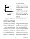
When power is turned on, the RESET output
U17, pin 6 is initially high and the inverted RESET
output U17, pin 5 is initially low. Once the 5V
supply stabilizes, these outputs remain in these states
for approximately 100 ms to ensure that reset occurs.
This time delay is set by capacitor C14 connected to
U17, pin 3. If the 5V supply drops below a nominal
level, the RESET outputs change states and micropro-
cessor operation is interrupted until the 5V supply re-
turns to normal. C3 prevents fast transients on the 5V
supply from causing reset.
Manual reset can be accomplished by pressing
push-button switch S1. When U17, pin 2 goes low,
U17 goes into the reset sequence described.


