


8-1
March 1999
Part No. 001-2009-600
SECTION 8 SERVICING
8.1 INTRODUCTION
8.1.1 PERIODIC CHECKS
This repeater should be put on a regular mainte-
nance schedule and an accurate performance record
maintained. Important checks are receiver sensitivity
and transmitter frequency, modulation, and power out-
put. It is recommended that repeater performance be
checked regularly even though periodic checks are not
specifically required by the FCC.
8.1.2 SURFACE-MOUNTED COMPONENTS
A large number of the components used in this
repeater are the surface-mounted type. Since these
components are relatively small in size and are sol-
dered directly to the PC board, care must be used
when they are replaced to prevent damage to the com-
ponent or PC board. Surface-mounted components
should not be reused since they may be damaged by
the unsoldering process. For more information on
replacing surface-mounted components, refer to the
Surface-Mounted Device Handbook, Part No. 001-
0576-002.
8.1.3 SCHEMATIC DIAGRAMS AND COMPO-
NENT LAYOUTS
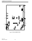
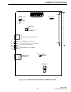
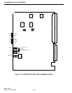
Schematic diagrams and component layouts of
the PC boards used in this repeater are located in Sec-
tion 10. A component locator guide is also provided
for both the schematic and board layouts to aid in
component location.
8.1.4 REPLACEMENT PARTS LIST
A replacement parts list containing all the parts
used in this repeater is located in Section 9. Parts are
listed alpha numerically according to designator. For
information on ordering parts, refer to Section 1.10.
8.1.5 TCXO MODULES NOT SERVICEABLE
Transmit or Receive TCXOs are not field ser-
viceable because if a part is changed, a factory recali-
bration must be performed to ensure that it stays
within its ±1 PPM tolerance.
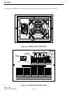
8.2 SYNTHESIZER SERVICING
8.2.1 INTRODUCTION
Synthesizer malfunctions can be caused by no
VCO output, or the VCO is unlocked. The VCO can
be unlocked due to a bad synthesizer chip, an incom-
plete synthesizer phase-lock loop, or because the syn-
thesizer chip is programmed incorrectly.
To make certain that the synthesizer chip is
receiving programming data, pins 17, 18 and 19 of the
chip should be monitored during programming. Pin
17 (Enable
) will go from a high to a low level. Pin 18
(Clock) will go from low to high in narrow pulses.
Pin 19 (Data) goes from high to low with wider data
pulses.
When the VCO is locked, the lock detect line of
the synthesizer pin 2 is high with very narrow nega-
tive-going pulses. These pulses become wider when
the VCO is out of lock. When this unlock condition
exists either in the Exciter VCO or the Receiver VCO
it is relayed by the RF Interface board and is detected
by the MPC via the RF Data lines. The MPC then
does not allow the transmitter to key and the receiver
cannot unsquelch.
When the VCO is unlocked, the f
R and fV inputs
to the phase detector are not in phase (refer to Sections
6.1.15 and 6.2.8). The phase detector in the synthe-
sizer then causes the VCO control voltage to go to the
high or low end of its operating range (0 or 9V). This
in turn causes the VCO to oscillate at the high or low
end of its frequency range.
As shown in Figures 6-1 and 6-4, a loop is
formed by the VCO, buffer, frequency input (F
IN) and
the phase detector output (PD OUT). Therefore, if
any of these components begin to malfunction,
improper signals appear throughout the loop. How-
ever, correct operation of the counters can still be veri-
fied by measuring the input and output frequencies to
check the divide number.
Proceed as follows to check the input and output
signal of the synthesizer modules to determine if they
are operating properly.