CIRCUIT DESCRIPTION
6-5
March 1999
Part No. 001-2009-600
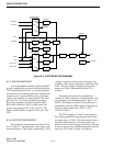
To determine the overall divide number of the
prescaler and N counter, the number of TCXO output
pulses required to produce one N counter output pulse
can be counted. The prescaler divides by 65 for 65 x
22 or 1430 input pulses. It then divides by 64 for 64 x
(27 - 22) or 320 input pulses. The overall divide num-
ber K is therefore (320 + 1430) or 1750. The TCXO
frequency of 17.5000 MHz divided by 1750 equals 10
kHz which is the fR input to the phase detector. The
overall divide number K can also be determined by
the formula:
K = 64N + A
Where, N = N counter divide number
A = A counter divide number.
6.1.10 LOCK DETECT
When the synthesizer is locked on frequency, the
Lock Detect output on U205, pin 2 is a logic high
voltage with narrow negative-going pulses. When the
synthesizer is unlocked, the negative- going pulses are
much wider, the width may vary at a rate determined
by the frequency difference of fV and fR. The lock
detect pulses are applied to J201, pin 19 and sent to
the RF Interface on J102, pin 19 for detection and
sampling in the IAC.
6.1.11 BUFFER AMPLIFIER
A cascode amplifier formed by Q206 and Q207
provides amplification and also isolation between the
TCXO and Synthesizer U205. A cascode amplifier is
used because it provides high reverse isolation. The
input signal to this amplifier is from TCXO Y201.
C250 provides DC blocking. Bias for the amplifier is
provided by R241, R242, R243, R244 and R240.
L217 is an RF choke. RF bypass is provided by C244,
C249 and C248. The output of Q206/Q207 is coupled
to U205 by C306
6.1.12 VCO (A006)
The VCO (Voltage-Controlled Oscillator) is
formed by Q802 circuitry and a resonator consisting
of L220 in the Receiver. The adjusting screw in L220
tunes the tank circuit to the desired frequency range.
The VCO oscillates in a frequency range from
843-848 MHz. Biasing of Q802 is provided by R805,
R806 and R807. AC voltage divider C812 and C813
initiates and maintains oscillation. C803 couples
Q802 to resonator L220 that provides the shunt induc-
tance of the tank circuit. The shunt capacitance of the
tank circuit is made primarily by C804 in series with
CR802.
The VCO frequency is controlled by a DC volt-
age across varactor diode CR802. As voltage across a
reverse-biased varactor diode increases, its capaci-
tance decreases. Therefore, VCO frequency increases
as the control voltage increases. The control line is
RF isolated from tank circuit by choke L804. The
amount of frequency change produced by CR802 is
controlled by series capacitor C804.
6.1.13 ACTIVE FILTER
Q801 functions as a capacitance multiplier to
provide filtering of the 12V supply to Q802. R801
and R802 provide transistor bias, and C809 provides
the capacitance that is effectively multiplied by the
gain of Q801. If a noise pulse or other voltage change
appears on the collector, the base voltage does not
change because of C809. Therefore, the base current
does not change and transistor current remains con-
stant. R803 decouples the VCO output from AC
ground. L803 is an RF choke and C807, C808, C810
and C811 provide RF bypass.
6.1.14 BUFFER
A cascode amplifier formed by Q208/Q209 pro-
vides amplification and isolation between the VCO
and synthesizer. A cascode amplifier is used because
it provides high gain, high isolation and consumes
only a small amount of power. The input signal to this
amplifier is coupled from the VCO RF output on
pin 4. DC blocking to the VCO is provided by C268
and to the buffer by C261. Bias for the amplifier is
provided by R275, R279, R278 and R277. Q209 is a
common-emitter amplifier and Q208 is a common-
base with C260 providing RF bypass. L219 provides
some filtering of the cascode output. R273 lowers the
Q of L219. The output of the amplifier is coupled by
C309 to U209, pin 11.


