


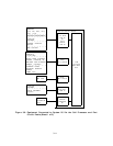
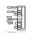
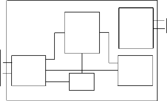
Memory Circuit Pack (ZTN81 or ZTN127)
The Memory Circuit Pack provides for the storage of software associated with system
operation. This software includes call and administration processing, and other related
programs. The circuit pack is powered from the backplane by +5 volts. Each system must
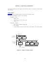
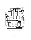
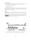
include one Memory Circuit Pack. The Memory Circuit Pack circuitry (Figure 3-3) includes:
● Address and data buffers
● ROM array
● ROM select
● Timing and control logic
● Built-in TDM bus termination resistors.
Address and Data Buffers: The address and data buffers interface the Memory Circuit
Pack to the address and data lines on the front plane.
ROM Array: The memory array consists of 16 ROM devices of 32K, 8 bit bytes each, for a
total capacity of 512K ROM. The ROMs are organized into pairs allowing the Call Processor
to access 16 bit words.
ROM Select:
The memory selects the proper pair of ROMs according to address
information.
Timing and Control Logic Circuit:
Controls the access speed of the ROM (no wait
states) by returning a Data Transfer Acknowledge signal at the proper time.
Bus Terminators: These resistors are required for proper operation of the TDM bus. The
Memory Circuit Pack provides the proper termination for one end of the bus, and a plug-in
TDM bus termination circuit card (plugs into cabinet backplane) is used to terminate the
other end. For this reason, the Memory Circuit Pack must always be located in slot #l of
Cabinet 1.
/
ADDRESS
AND
ROM
DATA BUFFERS
TIMING
ARRAY
AND
CONTROL
\
/
FRONT PANEL
MEMORY BUS
(TO CALL
PROCESSOR
CIRCUIT
PACK )
TERMINATOR
ROM
RESISTORS
SELECT
TO
TDM
BUS
\
Figure 3-3. Memory (ZTN81 or ZTN127) Circuitry
3-5