


98 www.xilinx.com PicoBlaze 8-bit Embedded Microcontroller
UG129 (v1.1.2) June 24, 2008
Appendix : PicoBlaze Instruction Set and Event Reference
R
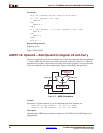
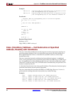
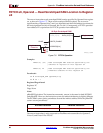
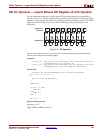
FETCH sX, Operand — Read Scratchpad RAM Location to Register
sX
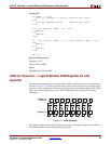
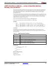
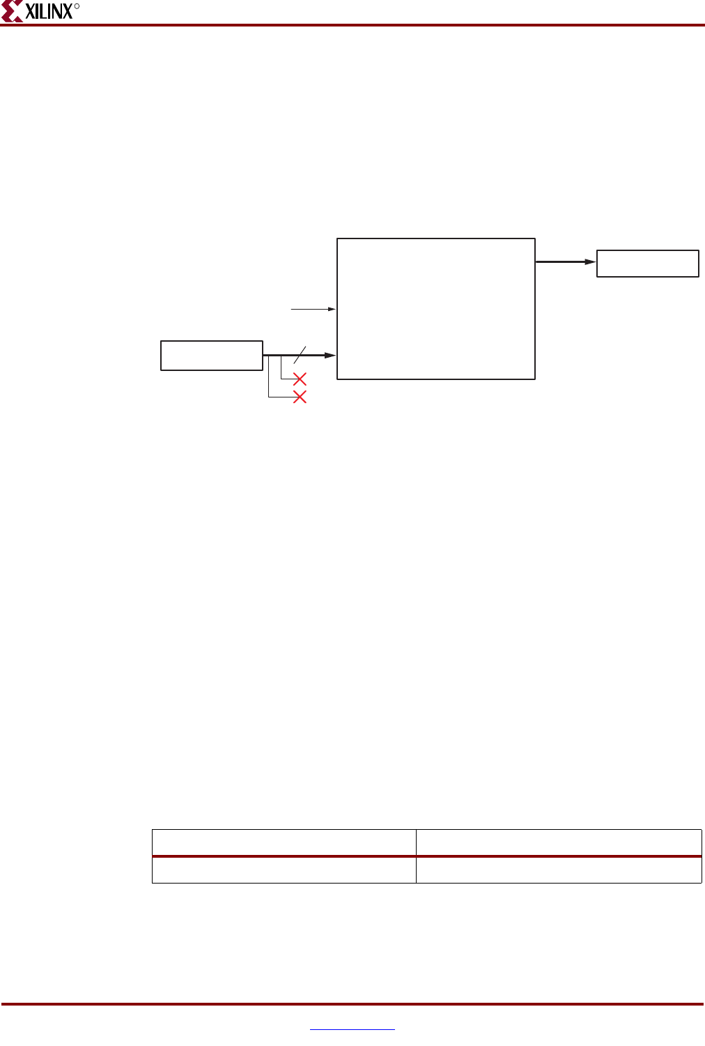
The FETCH instruction reads scratchpad RAM location specified by Operand into register
sX, as shown in Figure C-5. There are 64 scratchpad RAM locations. The two most-
significant bits of Operand, bits 7 and 6, are discarded and the RAM address is truncated to
the least-significant six bits of Operand, bits 5 to bit 0. Consequently, a FETCH operation
from address FF is equivalent to a FETCH operation from address 3F.
Examples
FETCH sX, (sY) ; Read scratchpad RAM location specified by the
; contents of register sY into register sX
FETCH sX, kk ; Read scratchpad RAM location specified by the
; immediate constant kk into register sX
Pseudocode
sX Å Scratchpad_RAM [Operand[5:0]]
PC Å PC + 1
Registers/Flags Altered
Registers: PC
Flags: None
Notes
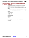
pBlazIDE Equivalent: The instruction mnemonic, FETCH, is the same for both KCPSM3
and pBlazIDE. However, the instruction syntax for indirect addressing is slightly different.
The KCPSM3 syntax places parentheses around the indirect address while the pBlazIDE
syntax uses no parentheses.
The FETCH instruction is only supported on PicoBlaze microcontrollers for Spartan-3,
Virtex-II, and Virtex-II Pro FPGAs.
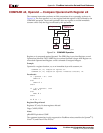
Figure C-5: FETCH Operation
KCPSM3 Instruction PBlazIDE Instruction
FETCH sX, (sY) FETCH sX, sY
Register sY or
Literal kk
Register sX
DATA_IN[7:0]
ADDRESS[5:0]
DATA_OUT[7:0]
64-Byte Scratchpad RAM
WRITE_ENABLEFALSE
[5:0]
[7]
[6]
UG129_aC_11_051604