


PicoBlaze 8-bit Embedded Microcontroller www.xilinx.com 59
UG129 (v1.1.2) June 24, 2008
R
Chapter 7
Instruction Storage Configurations
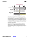
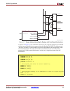
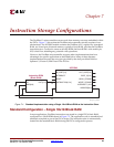
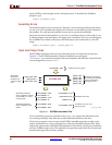
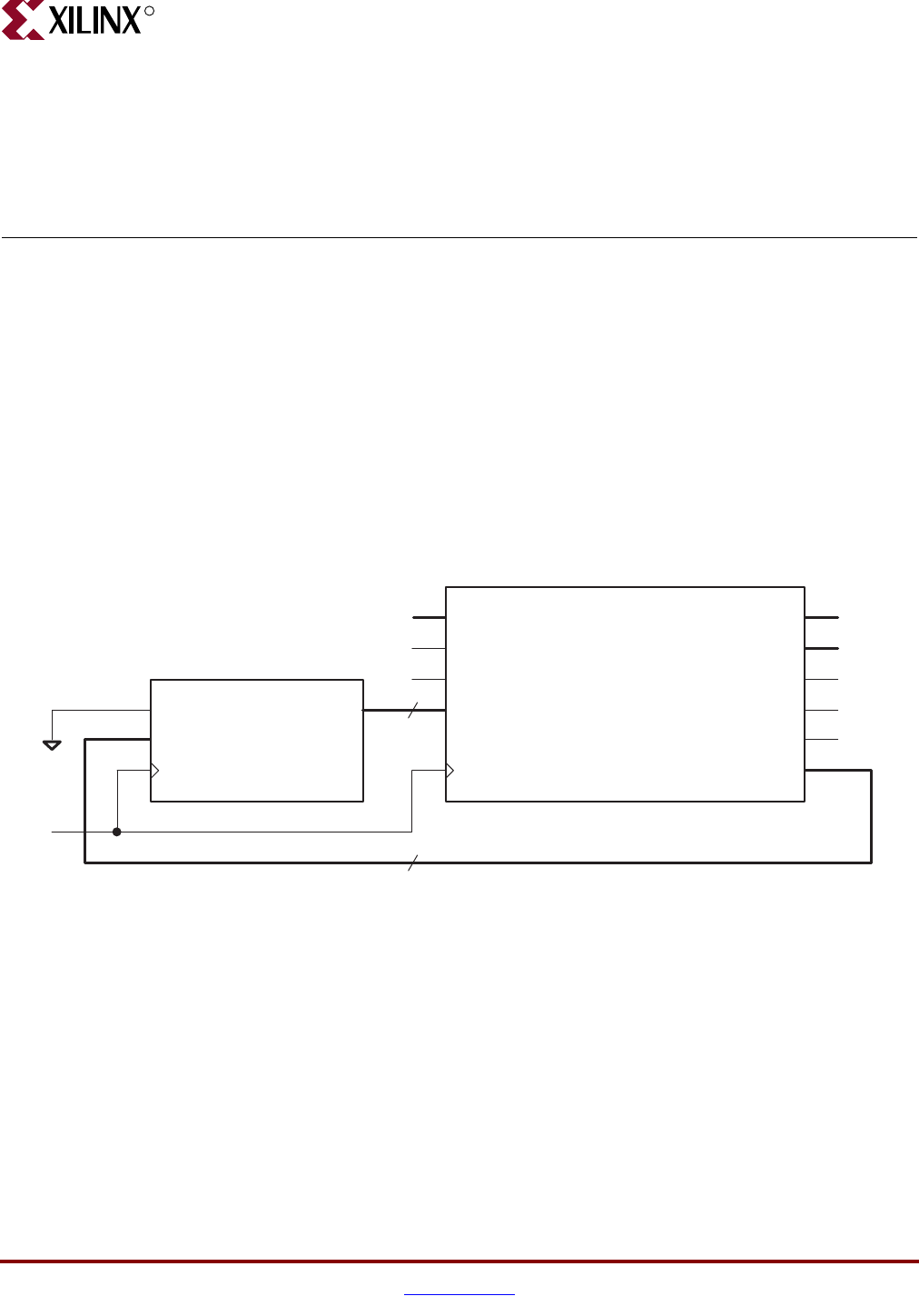
The PicoBlaze™ microcontroller executes code from memory resources embedded within
the FPGA. Figure 7-1 shows that the PicoBlaze microcontroller actually consists of two
subfunctions. The KCPSM3 module contains the PicoBlaze ALU, register file, scratchpad
RAM, etc. Some form of internal memory, typically a block RAM, provides the PicoBlaze
instruction store. To effective create an on-chip ROM, the block RAM’s write enable pin,
WE, is held Low, disabling any potential write operations.
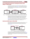
However, the PicoBlaze microcontroller supports other implementations that have
advantages for specific applications as described below. Many of these alternate
implementations leverage the extra port provided by the dual-port block RAM on
Spartan
®
-3, Virtex
®
-II, and Virtex-II Pro FPGAs.
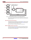
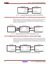
Standard Configuration – Single 1Kx18 Block RAM
In most applications, PicoBlaze instructions are stored in a single FPGA block RAM,
configured as a 1Kx18 ROM shown in Figure 7-2. The application code is assembled and
ultimately compiled as part of the FPGA design. The instruction store is automatically
loaded into the attached block RAM during the FPGA configuration process.
Figure 7-1: Standard Implementation using a Single 1Kx18 Block RAM as the Instruction Store
INSTRUCTION[17:0]
ADDRESS[9:0]
INTERRUPT_ACK
WRITE_STROBE
READ_STROBE
PORT_ID[7:0]
OUT_PORT[7:0]IN_PORT[7:0]
INTERRUPT
RESET
KCPSM3
ADDR[9:0]
OUT[17:0]
Instruction ROM
(Block RAM)
WE
18
10
UG129_c7_01_051504