


12 www.xilinx.com PicoBlaze 8-bit Embedded Microcontroller
UG129 (v1.1.2) June 24, 2008
Chapter 1: Introduction
R
• Byte-wide Arithmetic Logic Unit (ALU) with CARRY and ZERO indicator flags
• 64-byte internal scratchpad RAM
• 256 input and 256 output ports for easy expansion and enhancement
• Automatic 31-location CALL/RETURN stack
• Predictable performance, always two clock cycles per instruction, up to 200 MHz or
100 MIPS in a Virtex-II Pro FPGA
• Fast interrupt response; worst-case 5 clock cycles
• Optimized for Xilinx Spartan-3, Virtex-II, and Virtex-II Pro FPGA architectures—just
96 slices and 0.5 to 1 block RAM
• Assembler, instruction-set simulator support
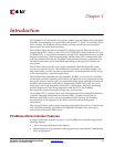
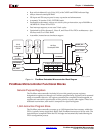
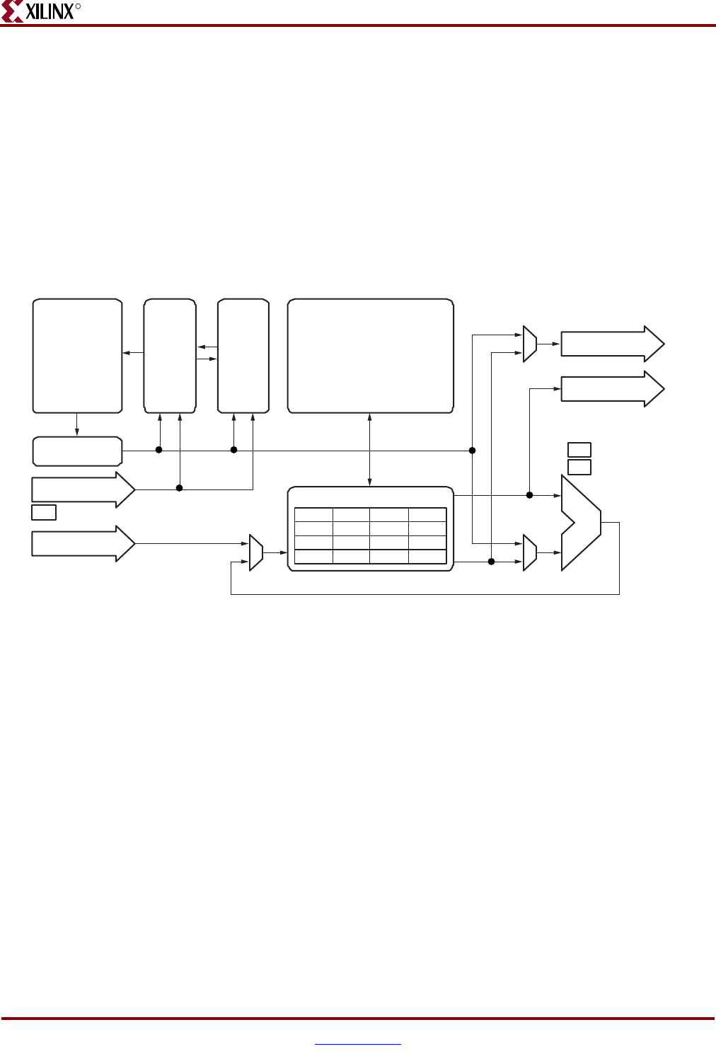
PicoBlaze Microcontroller Functional Blocks
General-Purpose Registers
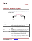
The PicoBlaze microcontroller includes 16 byte-wide general-purpose registers,
designated as registers s0 through sF. For better program clarity, registers can be renamed
using an assembler directive. All register operations are completely interchangeable; no
registers are reserved for special tasks or have priority over any other register. There is no
dedicated accumulator; each result is computed in a specified register.
1,024-Instruction Program Store
The PicoBlaze microcontroller executes up to 1,024 instructions from memory within the
FPGA, typically from a single block RAM. Each PicoBlaze instruction is 18 bits wide. The
instructions are compiled within the FPGA design and automatically loaded during the
FPGA configuration process.
Figure 1-1: PicoBlaze Embedded Microcontroller Block Diagram
s0 s1 s2 s3
s4 s5 s6 s7
s8 s9 sA sB
sC sD sE sF
Z
C
Zero
Carry
OUT_PORT
PORT_ID
IN_PORT
64-Byte
Scratchpad RAM
Instruction
Decoder
1Kx18
Instruction
PROM
INTERRUPT
16 Byte-Wide Registers
ALU
Operand 1
Operand 2
IE
Enable
Flags
Constants
UG129_c1_01_051204
Program Counter
(PC)
31x10
CALL/RETURN
Stack