


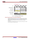
60 www.xilinx.com PicoBlaze 8-bit Embedded Microcontroller
UG129 (v1.1.2) June 24, 2008
Chapter 7: Instruction Storage Configurations
R
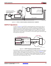
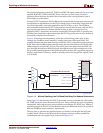
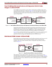
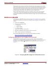
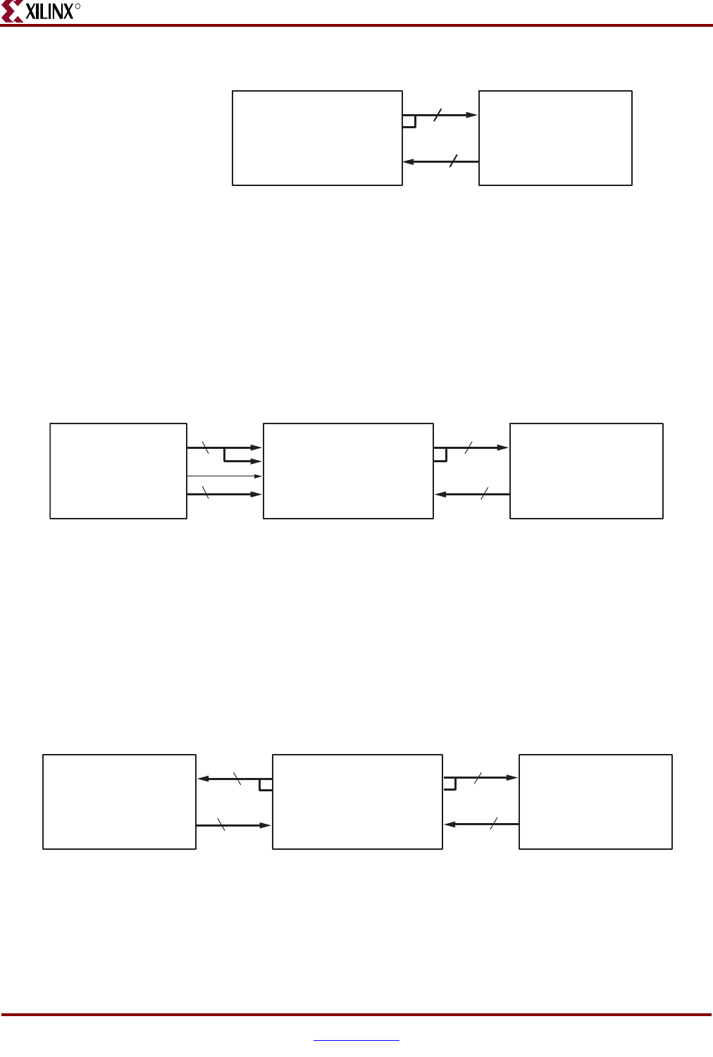
Standard Configuration with UART or JTAG Programming Interface
The second read/write port on the block RAM provides a convenient means to update the
PicoBlaze instruction store without recompiling the entire FPGA design. While the
processor is halted, application code can be updated via a simple UART or via the FPGA’s
JTAG port, as shown in Figure 7-3.
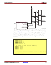
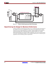
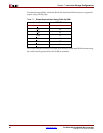
Two PicoBlaze Microcontrollers Share a 1Kx18 Code Image
As shown in Figure 7-4, two PicoBlaze microcontrollers can share a single dual-port block
RAM to store a common or mostly common code image. The two microcontrollers operate
entirely independently of one another although they each independently execute the same
or mostly the same code. The clock input, I/O ports, and interrupt input are unique to each
microcontroller.
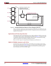
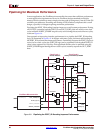
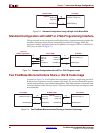
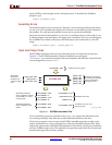
Figure 7-2: Standard Configuration using a Single 1Kx18 Block RAM
KCPSM3
ADDRESS[9:0]
INSTRUCTION[17:0]
ADDR[9:0]
DOP[1:0]
DO[15:0]
18
10
Block RAM
(1Kx18)
UG129_c7_02_051504
Figure 7-3: Standard Configuration with UART or JTAG Program Loader
KCPSM3
ADDRESS[9:0]
INSTRUCTION[17:0]
ADDRB[9:0]
DOPB[1:0]
DOB[15:0]
18
10
DIPA[1:0]
DIA[15:0]
ADDRA[9:0]
WEA
18
10
UART or
JTAG Programmer Block RAM
(1Kx18)
UG129_c7_03_051504
Figure 7-4: Two PicoBlaze Microcontrollers Sharing a Common Code Image
10
18
10
Block RAM
ADDRB[9:0]
DOPB[1:0]
DOB[15:0]
DOPA[1:0]
DOA[15:0]
ADDRA[9:0]
KCPSM3
ADDRESS[9:0]
INSTRUCTION[17:0]
KCPSM3
ADDRESS[9:0]
INSTRUCTION[17:0]
18
(1Kx18)
UG129_c7_04_051804