


PicoBlaze 8-bit Embedded Microcontroller www.xilinx.com 61
UG129 (v1.1.2) June 24, 2008
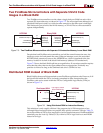
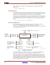
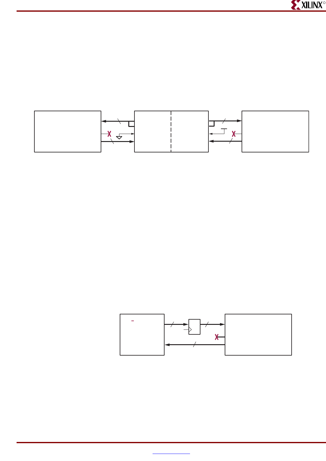
Two PicoBlaze Microcontrollers with Separate 512x18 Code Images in a Block RAM
R
Two PicoBlaze Microcontrollers with Separate 512x18 Code
Images in a Block RAM
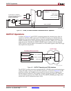
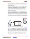
Two PicoBlaze microcontrollers can also share a single dual-port RAM but each with a
separate 512-instruction area, as shown in Figure 7-5. The most-significant address bit of
one block RAM port is tied Low while the other same bit on the other port is tied High.
This limits each port to half of the 1Kx18 memory, or 512x18. The two microcontrollers
operate independently.
Despite that both PicoBlaze microcontrollers use half the normal instruction store, the
interrupt vectors for both remain the same. When an interrupt occurs, the associated
KCPSM3 block presents all ones on the ADDRESS bus, which is truncated to the last
memory location in its half of the block RAM memory (address 1FF hexadecimal).
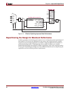
Figure 7-5 shows the block RAM split into two equal halves. If one microcontroller requires
more than the other, then tie the upper address lines as appropriate. Practically any
partition is allowed as long as the combined code size is 1,024x18 or less.
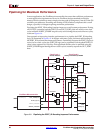
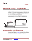
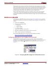
Distributed ROM Instead of Block RAM
Block RAM is the most efficient method to store PicoBlaze application code. However, if all
the block RAM within the FPGA is already committed to other functions then the
PicoBlaze code can be stored within the FPGAs Configurable Logic Blocks (CLBs), as
shown in Figure 7-6.
This technique is only roughly efficient if the program size is 128 instructions or less.
Although larger instruction stores are possible, they quickly consume CLB logic. Table 7-1
shows the number of FPGA slices required for various instruction stores. Distributed ROM
essentially uses the Look-Up Tables (LUTs) within its FPGA logic block as a small ROM
instead of for logic.
Figure 7-5: Two PicoBlaze Microcontrollers with Separate 512-Instruction Memory in one Block RAM
18
9
18
9
Block RAM
ADDRB[8:0]
DOPB[1:0]
DOB[15:0]
DOPA[1:0]
DOA[15:0]
ADDRA[8:0]
KCPSM3
ADDRESS[8:0]
INSTRUCTION[17:0]
KCPSM3
ADDRESS[8:0]
INSTRUCTION[17:0]
ADDRESS[9] ADDRA[9]
ADDRB[9] ADDRESS[9]
(512x18) (512x18)
UG129_c7_05_051504
Figure 7-6: Using Distributed ROM for Instruction Memory
KCPSM3
ADDRESS[5:0]
INSTRUCTION[17:0]
6
ADDRESS[9:6]
1818
Distributed ROM
ADDR[5:0]
O[17:0]
(<128x18)
Flip-flops to match
block RAM timing
UG129_c7_06_060404