


PicoBlaze 8-bit Embedded Microcontroller www.xilinx.com 13
UG129 (v1.1.2) June 24, 2008
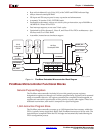
PicoBlaze Microcontroller Functional Blocks
R
Other memory organizations are possible to accommodate more PicoBlaze controllers
within a single FPGA or to enable interactive code updates without recompiling the FPGA
design. See Chapter 7, “Instruction Storage Configurations,” for more information.
Arithmetic Logic Unit (ALU)
The byte-wide Arithmetic Logic Unit (ALU) performs all microcontroller calculations,
including:
• basic arithmetic operations such as addition and subtraction
• bitwise logic operations such as AND, OR, and XOR
• arithmetic compare and bitwise test operations
• comprehensive shift and rotate operations
All operations are performed using an operand provided by any specified register (sX).
The result is returned to the same specified register (sX). If an instruction requires a second
operand, then the second operand is either a second register (sY) or an 8-bit immediate
constant (kk).
Flags
ALU operations affect the ZERO and CARRY flags. The ZERO flag indicates when the
result of the last operation resulted in zero. The CARRY flag indicates various conditions,
depending on the last instruction executed.
The INTERRUPT_ENABLE flag enables the INTERRUPT input.
64-Byte Scratchpad RAM
The PicoBlaze microcontroller provides an internal general-purpose 64-byte scratchpad
RAM, directly or indirectly addressable from the register file using the STORE and FETCH
instructions.
The STORE instruction writes the contents of any of the 16 registers to any of the 64 RAM
locations. The complementary FETCH instruction reads any of the 64 memory locations
into any of the 16 registers. This allows a much greater number of variables to be held
within the boundary of the processor and tends to reserve all of the I/O space for real
inputs and output signals.
The six-bit scratchpad RAM address is specified either directly (ss) with an immediate
constant, or indirectly using the contents of any of the 16 registers (sY). Only the lower six
bits of the address are used; the address should not exceed the 00 - 3F range of the available
memory.
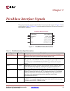
Input/Output
The Input/Output ports extend the PicoBlaze microcontroller’s capabilities and allow the
microcontroller to connect to a custom peripheral set or to other FPGA logic. The PicoBlaze
microcontroller supports up to 256 input ports and 256 output ports or a combination of
input/output ports. The PORT_ID output provides the port address. During an INPUT
operation, the PicoBlaze microcontroller reads data from the IN_PORT port to a specified
register, sX. During an OUTPUT operation, the PicoBlaze microcontroller writes the
contents of a specified register, sX, to the OUT_PORT port.
See Chapter 6, “Input and Output Ports,” for more information.