


PicoBlaze 8-bit Embedded Microcontroller www.xilinx.com 53
UG129 (v1.1.2) June 24, 2008
OUTPUT Operations
R
OUTPUT Operations
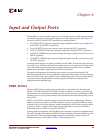
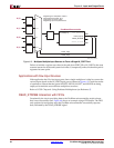
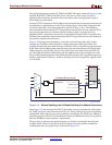
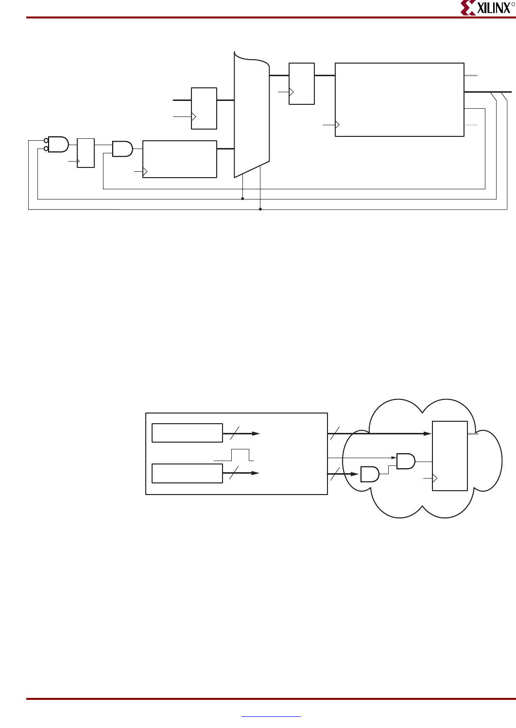
As shown in Figure 6-5, an OUTPUT operation presents the contents of any of the 16
registers to the OUT_PORT output port. The PORT_ID output port, defined either by
register sY or an 8-bit immediate constant, selects the desired output destination. The
WRITE_STROBE output pulse indicates that data on the OUT_PORT port is valid and
ready for capture. Typically, the WRITE_STROBE signal, combined with the decoded
PORT_ID port, is used as either a clock enable or a write enable signal to other FPGA logic
that captures the output data.
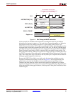
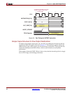
The OUTPUT operation asserts the associated WRITE_STROBE output pulse beginning on
rising CLK edge 1 of the two-cycle OUTPUT instruction , as shown in Figure 6-6. In this
particular example, the PicoBlaze microcontroller writes the contents of register s0 to
hexadecimal port address 65. The contents of register s0 appear on the OUT_PORT port;
the port address appears on the PORT_ID port. The WRITE_STROBE goes High on the
second clock cycle to indicate that data is valid.
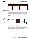
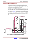
Figure 6-4: READ_STROBE Indicates a Successful INPUT Operation
IN_PORT[7:0] OUT_PORT[7:0]
PORT_ID[7:0]
READ_STROBE
WRITE_STROBE
PicoBlaze Microcontroller
0 1
0 0
S1
S0
PORT_ID[0]
PORT_ID[1]
READ DATA_OUT
FIFO
READ_STROBE
If performance is adequate,
remove the flip-flip and combine
the READ_STROBE and
PORT_ID decode logic.
UG129_c6_04_060404
Figure 6-5: OUTPUT Operation and FPGA Interface
m
EN
D Q
FPGA Logic
n
WRITE_STROBE
OUT_PORT[7:0]
PORT_ID[7:0]
PicoBlaze Microcontroller
8
8
Register sY or
Literal kk
Register sX
UG129_c6_05_052004