


36 www.xilinx.com PicoBlaze 8-bit Embedded Microcontroller
UG129 (v1.1.2) June 24, 2008
Chapter 3: PicoBlaze Instruction Set
R
Moving Data
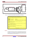
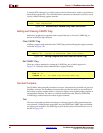
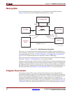
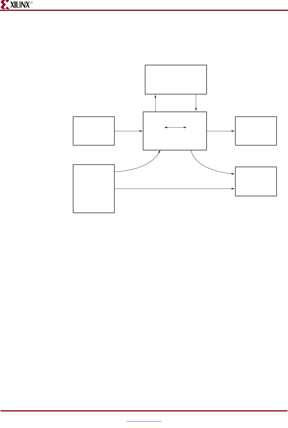
Data movement between various resources is an essential microcontroller function.
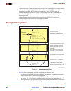
Figure 3-26 shows the various PicoBlaze instructions to move data.
The LOAD sX,sY instruction moves data between two PicoBlaze registers; Register sX
receives the data. The LOAD sX,kk instruction loads an immediate byte-wide constant into
the specified register. See also “LOAD sX, Operand — Load Register sX with Operand,”
page 102. The LOAD instructions do not affect the CARRY or ZERO flags.
The STORE and FETCH instructions move data between the register file and the scratchpad
RAM. See “Chapter 5, “Scratchpad RAM,” for more information.
During an INPUT operation, data from the IN_PORT input port is always read to one of the
registers. Likewise, during an OUTPUT instruction, data written to the OUT_PORT output
port always originates from one of the registers. The input/output address, provided on
the PORT_ID output, originates either from one of the registers or as a literal constant from
the instruction store. See Chapter 6, “Input and Output Ports,” for more information.
Program Flow Control
The Program Counter (PC) points to the next instruction to be executed and directly
controls the PicoBlaze program flow. By default, the PicoBlaze microcontroller proceeds to
the next instruction in the instruction store (PC=PC+1). The PC cannot be directly accessed.
However, three different PicoBlaze instructions, JUMP and the CALL/RETURN pair
potentially modify the default program flow by loading the PC with a different value. An
enabled interrupt event also modifies program flow but this case is described in Chapter 4,
“Interrupts.” Likewise, a Reset Event resets the PC to zero, restarting program execution.
Figure 3-26: Data Movement Instructions
Registers
LOAD sX, sY
Scratchpad RAM
FETCHSTORE
IN_PORT
INPUT
OUT_PORT
OUTPUT
PORT_ID
Instruction
Store
LOAD sX, kk
INPUT sX, (sY)
OUTPUT sX, (sY)
INPUT sX, kk
OUTPUT sX, kk
UG129_c3_05_060404