


PicoBlaze 8-bit Embedded Microcontroller www.xilinx.com 51
UG129 (v1.1.2) June 24, 2008
INPUT Operations
R
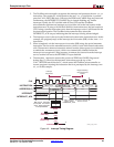
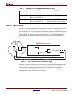
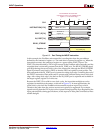
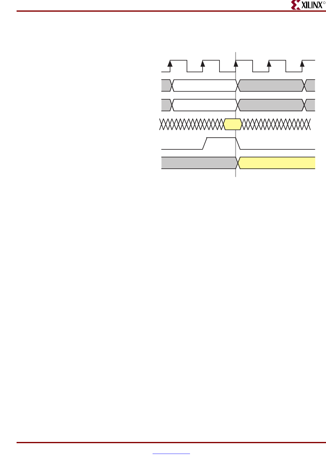
In this example, the PicoBlaze microcontroller is reading data from the port address
defined by the contents of register s7. The read data is captured in register s0. When the
instruction executes, the contents of register S7 appear on the PORT_ID port. The
PORT_ID is then decoded by FPGA logic external to the PicoBlaze microcontroller and the
requested data is eventually presented on the IN_PORT port. The READ_STROBE signal
goes High during the second clock cycle of the instruction, although the READ_STROBE
signal is primarily used only by FIFOs so that the FIFO can update its read pointer. The
data presented on the IN_PORT port is captured on rising clock edge 2, marking the end of
the INPUT instruction. Data needs only be present with sufficient setup time to this clock
edge. After rising clock edge 2, the data on the IN_PORT port is captured and available in
the target register, register s0 in this case.
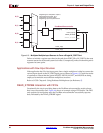
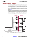
Because the PORT_ID is valid for two clock cycles, the input data multiplexer can be
registered to maintain performance, as shown in Figure 6-3. In most applications, the
actual clock cycle when the PicoBlaze microcontroller reads an input is not critical.
Therefore the paths from the various sources can typically be registered. For example,
signals arriving from the FPGA pins can be captured using input flip-flops. Registering the
input path simplifies timing specifications, avoids reports of ‘false paths’ and leads to more
reliable designs.
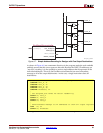
Figure 6-2: Port Timing for INPUT Instruction
INPUT s0,(s7)
Contents of
register s7
CLK
PORT_ID[7:0]
IN_PORT[7:0]
READ_STROBE
INSTRUCTION[17:0]
Register s0
Captured Value from
IN_PORT[7:0]
The PicoBlaze microcontroller
captures the value on IN_PORT[7:0] into
register s0 on this clock edge.
UG129_c6_02_060404
0
123
4