


PicoBlaze 8-bit Embedded Microcontroller www.xilinx.com 57
UG129 (v1.1.2) June 24, 2008
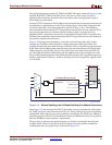
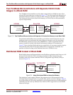
Pipelining for Maximum Performance
R
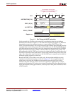
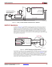
The pipelining registers on the OUT_PORT and PORT_ID signals, shaded in Figure 6-9, are
optional. Both OUT_PORT and PORT_ID are valid for two clock cycles. However,
pipelining them decreases the initial fanout and reduces the routing distance, both of
which improve performance.
During OUTPUT operations, the PicoBlaze microcontroller has no data dependencies and
consequently no dependencies on the FPGA interface logic. If data takes longer than the
two-clock instruction cycle to be captured by the FPGA logic, so be it. The PicoBlaze
microcontroller initiates the OUTPUT operation but does not need to wait while the FPGA
logic captures the data in its ultimate location as long as data is not lost. However,
pipelining INPUT operations can be more complicated. During an INPUT operation, the
PicoBlaze microcontroller requests data from the FPGA logic and must receive the data to
successfully complete the instruction.
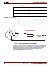
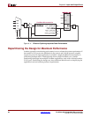
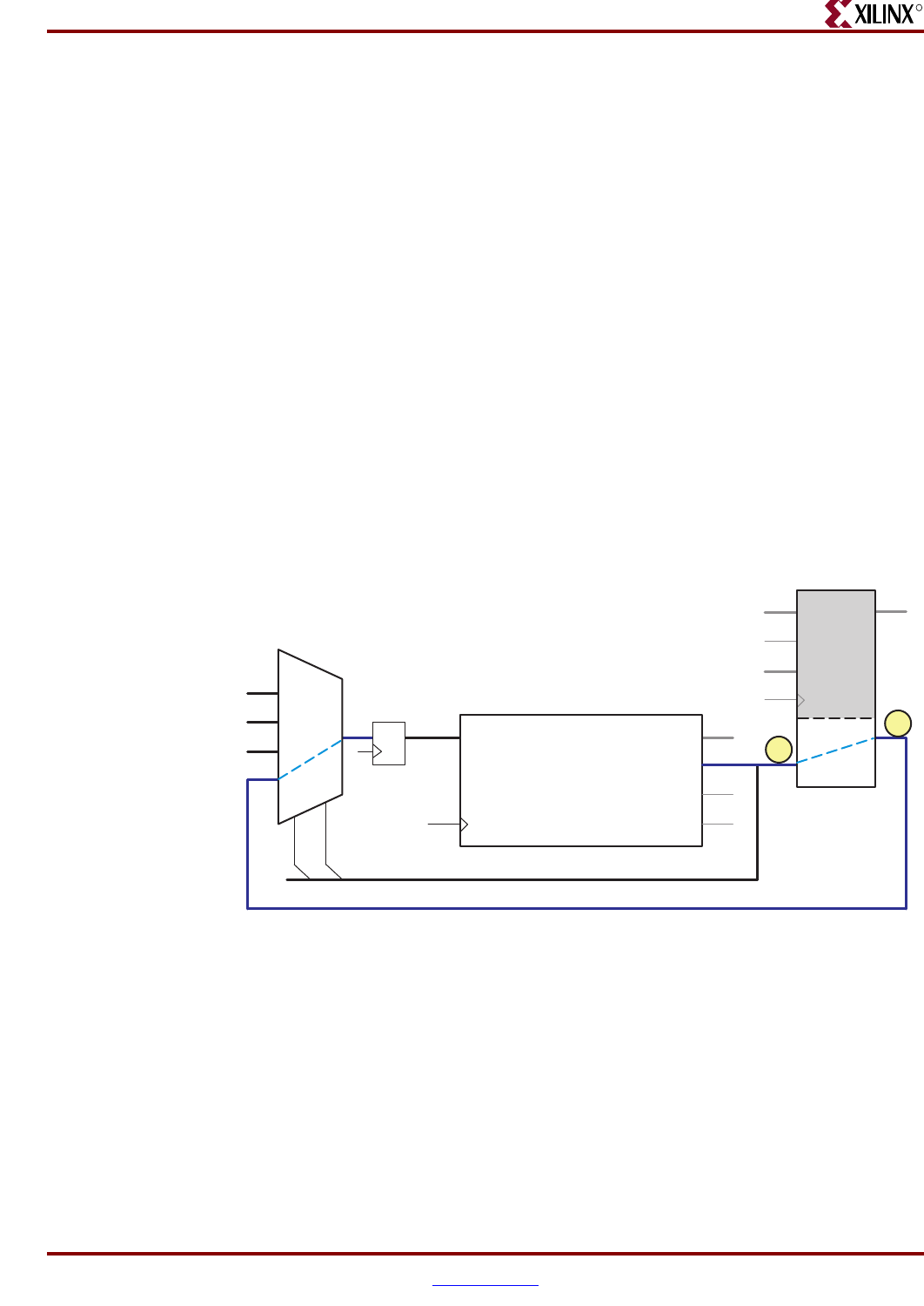
Figure 6-10 illustrates the dependency, where the critical timing path is blue. In this
example, the PicoBlaze microcontroller is reading data from a dual-port RAM. This
example assumes that some other function within the FPGA writes data into the dual-port
RAM. When the PicoBlaze microcontroller reads data from the dual-port RAM, the read
address appears on the PORT_ID port. The critical path is the delay from the PORT_ID
port, through the dual-port RAM read path, through the input select multiplexer, to the
setup on the pipelining register. If this path limits performance, add a pipelining register to
improve performance. However, where is the best position for the pipeline register, Point
A or Point B?
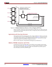
From Figure 6-2, the read data for INPUT operations must be presented and valid on the
IN_PORT port by the end of the second clock cycle. There is already one layer of pipelining
immediately following the input select multiplexer feeding the IN_PORT port. Adding a
pipelining register at Point A or Point B delays data by an additional clock cycle, too late to
meet the PicoBlaze microcontroller’s requirements.
The best place to position the pipeline register is at Point B, which splits the read path
roughly in half. However, the input select multiplexer structure must be modified to
accommodate the extra register layer, as shown in Figure 6-11.
Figure 6-10: Without Pipelining, the Full Read Path Delay Can Reduce Performance
IN_PORT[7:0] OUT_PORT[7:0]
PORT_ID[7:0]
READ_STROBE
WRITE_STROBE
PicoBlaze Microcontroller
WE
D SPO
A[4:0]
RAM16X1D (x8)
0 0
0 1
1 0
S1
S0
DPO
DPRA[4:0]
1 1
A
B
UG129_c6_09_052004