


52 www.xilinx.com PicoBlaze 8-bit Embedded Microcontroller
UG129 (v1.1.2) June 24, 2008
Chapter 6: Input and Output Ports
R
Failure to include a register anywhere in the path from PORT_ID to IN_PORT is the most
common reason for decreased system clock rates. Consequently, make sure that this path is
registered at some point.
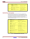
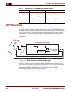
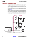
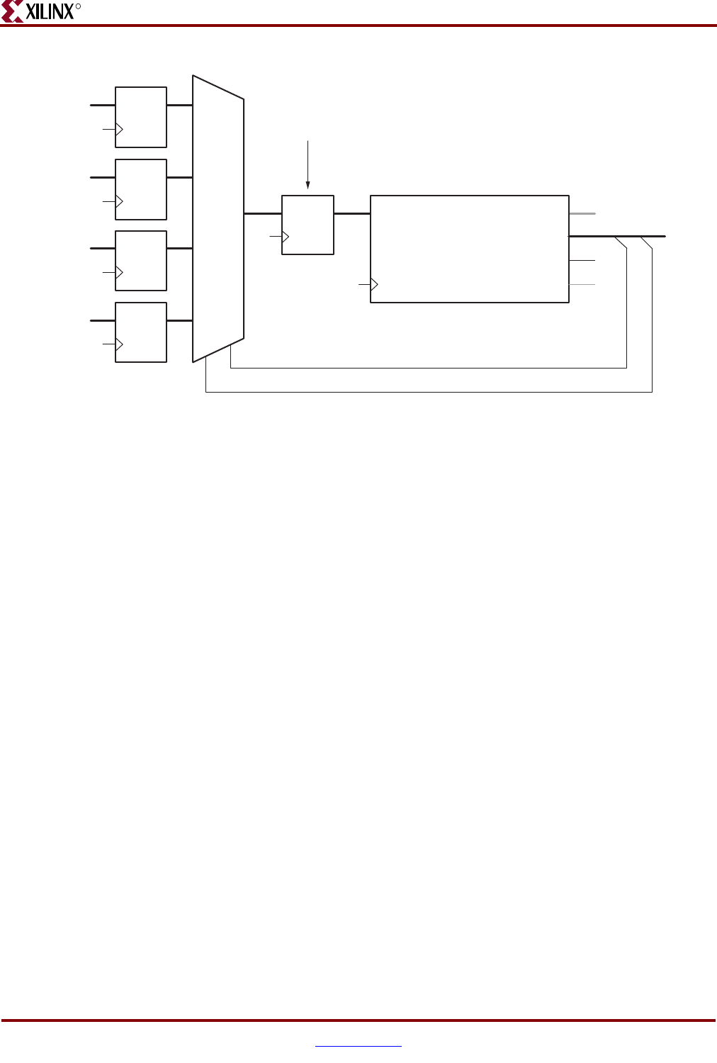
Applications with Few Input Sources
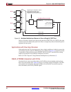
If the application has 32 or less input ports, then a single multiplexer is ideal to connect the
various input signals to the IN_PORT input port, as shown in Figure 6-3. Check the results
of synthesis to ensure that the special MUXF5, MUXF6, MUXF7, and MUXF8 are being
employed to make the most efficient multiplexer structure.
Refer to UG331 Chapter 8: Using Dedicated Multiplexers (see Reference 5).
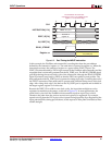
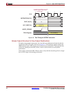
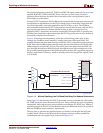
READ_STROBE Interaction with FIFOs
Occasionally, the circuit providing data to the PicoBlaze microcontroller needs to know
that it was successfully read. Figure 6-4 shows an example using a FIFO buffer. The FIFO
only updates its read pointer once the PicoBlaze microcontroller successfully captures
data, indicated by the READ_STROBE signal.
Figure 6-3: Multiplex Multiple Input Sources to Form a Single IN_PORT Port
IN_PORT[7:0] OUT_PORT[7:0]
PORT_ID[7:0]
READ_STROBE
WRITE_STROBE
PicoBlaze Microcontroller
1 1
1 0
0 1
0 0
S1
S0
PORT_ID[0]
PORT_ID[1]
IN_D
Registering the multiplexer output is
allowed because PORT_ID is
asserted for two clock cycles.
Registering improves performance.
IN_C
IN_B
IN_A
UG129_c6_03_060404