


CIRCUIT DESCRIPTION
4-5
November 1999
Part No. 001-7780-500
4.4.3 POWER CONTROL (IC2A/B)
The power output circuit maintains a steady
power output level by controlling the supply voltage to
the first stage in power module IC1 (VCC1). The
output power is monitored using a directional coupler
consisting of L34, L13, C33, C35, D4, D5, and several
other components. Reflected (reverse) power is
detected by L13/D5, and forward power is detected by
L12/D4. These couplers produce a DC voltage that is
proportional to the reverse or forward power.
The forward power signal is amplified by IC2A
and is combined with the reverse power signal on pin
6 of IC2B. If there is no reverse power being detected,
IC2B amplifies only the difference between the
forward power signal on pin 6 and the reference
voltage on pin 5. This reference voltage controls the
power output, and it is set by the control logic through
potentiometer 2 in IC209 in the logic unit.
As forward or reverse power increases, the output
voltage on pin 7 decreases. Q5 and Q6 then turn off
more which decreases the supply voltage applied to
VCC1 of IC1. Power then decreases to maintain a
stable output. The opposite occurs if forward or
reverse power decrease. The power decrease resulting
from an increase in reverse power prevents transmitter
damage which may result if excessive power is
reflected back into the transmitter. This may occur, for
example, if the transmitter is keyed with a defective
antenna.
4.5 CONTROL LOGIC AND DISPLAY
NOTE: A block diagram of the RF and logic units is
located on page 8-3.
4.5.1 CONTROL LOGIC
The digital control logic is based on 8-bit CMOS
microprocessor IC306. The operating speed is set by
9.8304 MHz crystal X2. A clock shift signal applied
through D301. This signal goes high to shift the clock
frequency slightly when the second harmonic inter-
feres with the receive signal.
A serial data bus formed by MSI, MSO, and
MSCK (pins 49-51) is used to transfer data to and
from two external devices. They are 16K x 8
EEPROM IC304 and DTMF encoder IC303. Another
serial port formed by XTXD and XRXD is used to
transfer programming data to and from an external
computer. This port is fed out of the transceiver on
pins 6 and 7 of the accessory connector. Descriptions
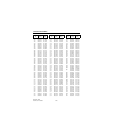
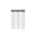
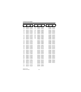
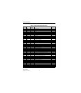
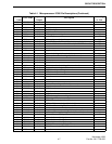
of the IC306 pins are located in Table 4-1.
4.5.2 DISPLAY ASSEMBLY DESCRIPTION
IC1 on the display board is an intelligent LCD
display controller/driver. It communicates with the
microprocessor on the logic board over a serial bus
consisting of MSCK (serial clock) and MSO (serial
data), and DISST (display strobe) signals. IC1 is set
for 1/3 bias and 1/5 duty cycle and drives an 8-char-
acter, 14-segment display at a 98 Hz frame frequency.
The LCD display (DS6) has 127 segments that are
driven by a 34-segment signal with 4 common lines.
4.6 RECEIVE AUDIO PROCESSING
4.6.1 BANDPASS FILTER (IC101)
The receive audio and data signal from the IF
module in the RF unit is called DET. It is applied to
IC101 in the receive audio circuit, IC102 in the receive
data circuit, and IC110 in the SMARTNET data
circuit. The receive audio circuit operates as follows,
and the other circuits are described in later sections.
The DET signal is applied to IC101 which is a
bandpass filter which passes frequencies from 300-
3000 Hz. This attenuates Call Guard (CTCSS/DCS)
signaling and high-frequency harmonics. This filter
also provides de-emphasis of the audio signal.
On the input of IC101, pin 1 of Q110 is low in the
wideband mode and high in the narrow band mode.
Therefore, R102 is grounded in the wideband mode to
lower the input level to IC101. This maintains a
constant audio output level since the higher deviation
in the wideband mode results in a higher input level.
Also on the input of IC101, the NPSPAC line control-
ling Q111 is high when a NPSPAC channel is selected
and low at other times. This grounds R167 in the
NPSPAC mode to lower the input level since NPSPAC
channel deviation is higher than narrow band
deviation.