


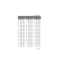
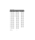
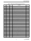

CIRCUIT DESCRIPTION
4-2
November 1999
Part No. 001-7780-500
the VCO from the receiver and transmitter and the
counters in synthesizer IC1.
A switching circuit on the output of Q10 routes
the VCO signal to the receiver in the receive mode and
the transmitter in the transmit mode. In the receive
mode, the R5V receive supply is applied to R12 and
current flows through R12, D7A, and R51. Since D7A
is forward biased, it presents a low impedance path to
first mixer Q2 in the receiver. D7C is then reverse
biased, so there is a high impedance path to the
transmitter.
The5VreceivesupplyisalsoappliedtoR78and
current flows through R78, D7B, and R79. This results
in less reverse bias and therefore charge on D7C to
permit faster switching. In the transmit mode, the 5V
receive supply is no longer present, so both D7A and
D7B are reverse biased. D7C is forward biased by the
current path through R50 and R51.
4.2.3 VCO AND TCXO MODULATION
Both the VCO and TCXO are modulated in order
to achieve the required frequency response. If only the
VCO was modulated, the phase detector in IC1 would
sense the frequency change and increase or decrease
the VCO control voltage to counteract the change
(especially at the lower audio frequencies).
Conversely, if only the TCXO was modulated, the
VCO frequency would not change fast enough (espe-
cially at the higher audio frequencies).
However, by modulating both the VCO and
TCXO, the two phase detector inputs remain in phase
and no frequency shift is sensed. This produces a rela-
tively flat audio response. Potentiometer B4 in IC209
is used to balance these signals and potentiometers B1
andB3areusedtosetthedataandaudiodeviation
level. IC4 is an amplifier, and R73 sets the frequency
of the TCXO by adjusting the DC bias of IC4.
4.2.4 SYNTHESIZER CHIP (IC1)
Synthesizer chip IC1 contains a prescaler, A, N,
and reference counters, and a phase detector. Chan-
nels are selected by programming the A, N, and refer-
ence counters to divide by a certain number. This
programming is performed by the microprocessor via
the serial data bus which consists of lines PLLSK,
PLLSO, and PLLST (pins 9-11 of IC1).
The divide numbers are chosen so that when the
VCO is operating at the correct frequency, the VCO-
derived input to the phase detector is the same
frequency as the TCXO-derived input. The TCXO-
derived input is produced by the reference counter in
IC1. This counter divides the 14.925 MHz TCXO
frequency by 2388 to produce a 6.25 kHz input to the
phase detector. Using a 6.25 kHz reference frequency
allows channels to be changed in 6.25 kHz steps.
The VCO-derived input is produced by dividing
the VCO frequency using the prescaler and N counter
in IC1. The divide number of the prescaler is
controlled by the output signal from the A counter.
The A and N counters function as follows:
Both the A and N counters begin counting down
from the programmed number. When the A counter
reaches zero, it halts until the N counter reaches zero.
Both counters then reset and the cycle repeats. The A
counter is always programmed with a smaller number
than the N counter. When the A counter is counting
down, the control output to the prescaler causes the
prescaler to divide by 129. Then when the A counter is
halted, the control output changes states and the pres-
caler divides by 128.
4.2.5 LOCK DETECT (Q13)
When the synthesizer is locked on frequency, the
LD (Lock Detect) output of IC1 (pin 7) is a high
signal. This turns lock detect transistor Q13 off and the
ULOCK signal fed to the microprocessor is low. When
an unlocked condition is indicated, low-going pulses
appear on pin 7. Q13 then turns on and the ULOCK
signal goes high. The transceiver is then disabled by
the logic and an error condition is indicated in the
display.
4.2.6 CHARGE PUMP (Q1, Q2), LOOP FILTER
The charge pump circuit consisting of Q1 and Q2
charges and discharges C4 and C5 in the loop filter to
produce the VCO control voltage. Supply voltage to
Q1 is provided by CPV regulator IC2 on the IF board.
Pulses which control the charge pump are output
by synthesizer IC1 on pins 15 and 16. When the VCO
is on the correct frequency, both phase detector
outputs are in phase. Pin 15 is then high and pin 16 is
low which turns both Q1 and Q2 off. Then if the VCO