


v
List of Illustrations
Figure Title Page
3–1 MCLKOUT Timing Diagram 3–1. . . . . . . . . . . . . . . . . . . . . . . . . . . . . . . . . . . . . . . . . . . . .
3–2 Microcontroller Interface Timing Requirements
(Mitsubishi Configuration Read Cycle, MTS [1:0] = 10) 3–2. . . . . . . . . . . . . . . . . . . . . .
3–3 Microcontroller Interface Timing Requirements
(Mitsubishi Configuration Write Cycle, MTS [1:0] = 10) 3–3. . . . . . . . . . . . . . . . . . . . . .
3–4 Microcontroller Interface Timing Requirements
(Intel Configuration Read Cycle, MTS [1:0] = 00) 3–4. . . . . . . . . . . . . . . . . . . . . . . . . . .
3–5 Microcontroller Interface Timing Requirements
(Intel Configuration Write Cycle, MTS [1:0] = 00) 3–5. . . . . . . . . . . . . . . . . . . . . . . . . . .
3–6 Microcontroller Interface Timing Requirements
(Motorola 16-Bit Read Cycle, MTS [1:0] = 10) 3–6. . . . . . . . . . . . . . . . . . . . . . . . . . . . . .
3–7 Microcontroller Interface Timing Requirements
(Motorola 16-Bit Write Cycle, MTS [1:0] = 10) 3–7. . . . . . . . . . . . . . . . . . . . . . . . . . . . . .
3–8 Microcontroller Interface Timing Requirements
(Motorola 8-Bit Read Cycle, MTS [1:0] = 01) 3–8. . . . . . . . . . . . . . . . . . . . . . . . . . . . . . .
3–9 Microcontroller Interface Timing Requirements
(Motorola 8-Bit Write Cycle, MTS [1:0] = 01) 3–9. . . . . . . . . . . . . . . . . . . . . . . . . . . . . . .
3–10 TCM4300 to DSP Interface (Read Cycle) 3–10. . . . . . . . . . . . . . . . . . . . . . . . . . . . . . . . . .
3–11 TCM4300 to DSP Interface (Write Cycle) 3–11. . . . . . . . . . . . . . . . . . . . . . . . . . . . . . . . . .
4–1 Power Ramp-Up/Ramp-Down TIming Diagram 4–6. . . . . . . . . . . . . . . . . . . . . . . . . . . . .
4–2 Transmit Power Ramp-Up/Ramp-Down Functional Diagram 4–7. . . . . . . . . . . . . . . . .
4–3 WBD Manchester-Coded Data Stream 4–9. . . . . . . . . . . . . . . . . . . . . . . . . . . . . . . . . . . .
4–4 Codec Master and Sample Clock Timing 4–12. . . . . . . . . . . . . . . . . . . . . . . . . . . . . . . . . .
4–5 Timing and Clock Generation for 38.88-MHz Clock 4–14. . . . . . . . . . . . . . . . . . . . . . . . .
4–6 Synthesizer Interface Circuit Block Diagram 4–16. . . . . . . . . . . . . . . . . . . . . . . . . . . . . . .
4–7 Contents of SynData Registers 4–17. . . . . . . . . . . . . . . . . . . . . . . . . . . . . . . . . . . . . . . . . .
4–8 Example Synthesizer Output 4–18. . . . . . . . . . . . . . . . . . . . . . . . . . . . . . . . . . . . . . . . . . . .
4–9 Internal and External Power Control Logic 4–19. . . . . . . . . . . . . . . . . . . . . . . . . . . . . . . . .
4–10 Microcontroller-DSP Data Buffers 4–20. . . . . . . . . . . . . . . . . . . . . . . . . . . . . . . . . . . . . . . .
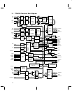
4–11 DSP Interface 4–26. . . . . . . . . . . . . . . . . . . . . . . . . . . . . . . . . . . . . . . . . . . . . . . . . . . . . . . . .
4–12 Power-On Reset Timing 4–28. . . . . . . . . . . . . . . . . . . . . . . . . . . . . . . . . . . . . . . . . . . . . . . . .