


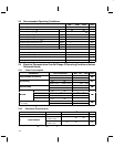
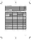
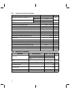
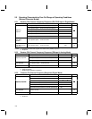

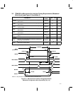
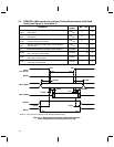
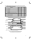
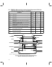
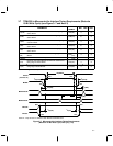
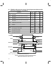
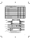
3–2
3.2 TCM4300 to Microcontroller Interface Timing Requirements (Mitsubishi
Read Cycle) (see Figure 3–2 and Note 2)
PARAMETER
ALTERNATE
SYMBOL
MIN MAX
UNIT
t
su(R/W)
Setup time, read/write MCRW stable before falling edge of
strobe MCDS
TRW
(SU)
0 ns
t
h(R/W)
Hold time, read/write MCRW stable after rising edge of
strobe MCDS
TRW
(HO)
10 ns
t
su(RA)
Setup time, read address MCS stable before falling edge of
strobe MCDS
TRA
(SU)
0 ns
t
h(RA)
Hold time, read address MCA stable after rising edge of
strobe MCDS
TRA
(HO)
10 ns
t
en(RD)
Enable time, read data on falling edge of strobe MCDS to
TCM4300 driving data bus MCD
TRD
(EN)
10 ns
t
v(R)
Read data valid time on falling edge of strobe MCDS to
valid data MCD
TRD
(DV)
50 ns
t
inv
Data MCD invalid after rising edge of strobe MCDS TRD
(INV)
10 ns
t
dis(RD)
Disable time, read data. TCM4300 releases MCD data bus
after rising edge of strobe MCDS
TRD
(DIS)
28 ns
t
h(CS)
Hold time, chip select MCCSH and MCCSL stable before
rising edge of strobe MCDS
TCS
(HO)
0 ns
t
su(CS)
Setup time, chip select MCCSH and MCCSL stable before
falling edge of strobe MCDS
TCS
(SU)
0 ns
NOTE 2: Timings are based upon Mitsubishi 37732S4 (16 MHz) and Mitsubishi 3772S4L (8 MHz).
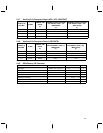
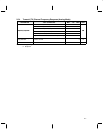
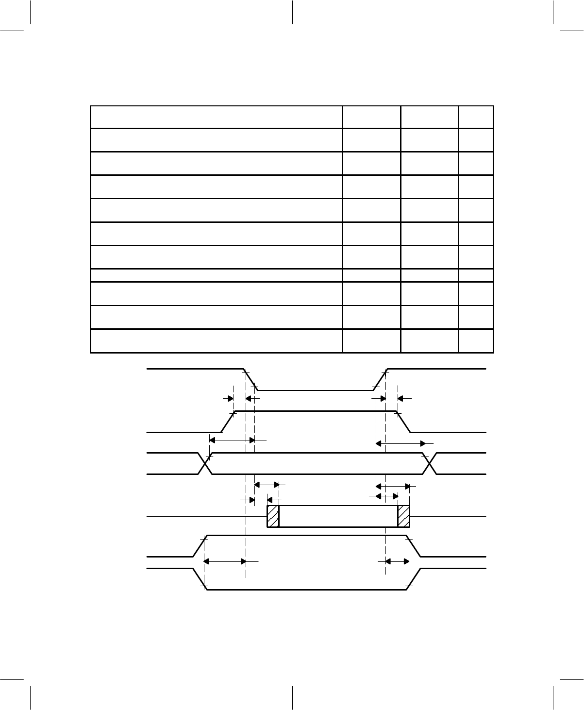
MCA4–MCA0
MCD7–MCD0
MCDS
(see Note A)
MCRW
10%
90%
90%
10%
90%90%
t
su(R/W)
t
v(R)
t
en(RD)
t
dis(RD)
t
inv
t
su(CS)
t
h(CS)
MCCSH
MCCSL
90% 90%
10% 10%
NOTE A: Chip selection is defined as both MCCS and MCDS active.
t
h(R/W)
t
su(RA)
t
h(RA)
Figure 3–2. Microcontroller Interface Timing Requirements
(Mitsubishi Configuration Read Cycle, MTS [1:0] = 10)