


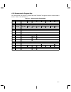
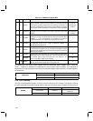
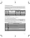
4–24
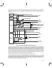
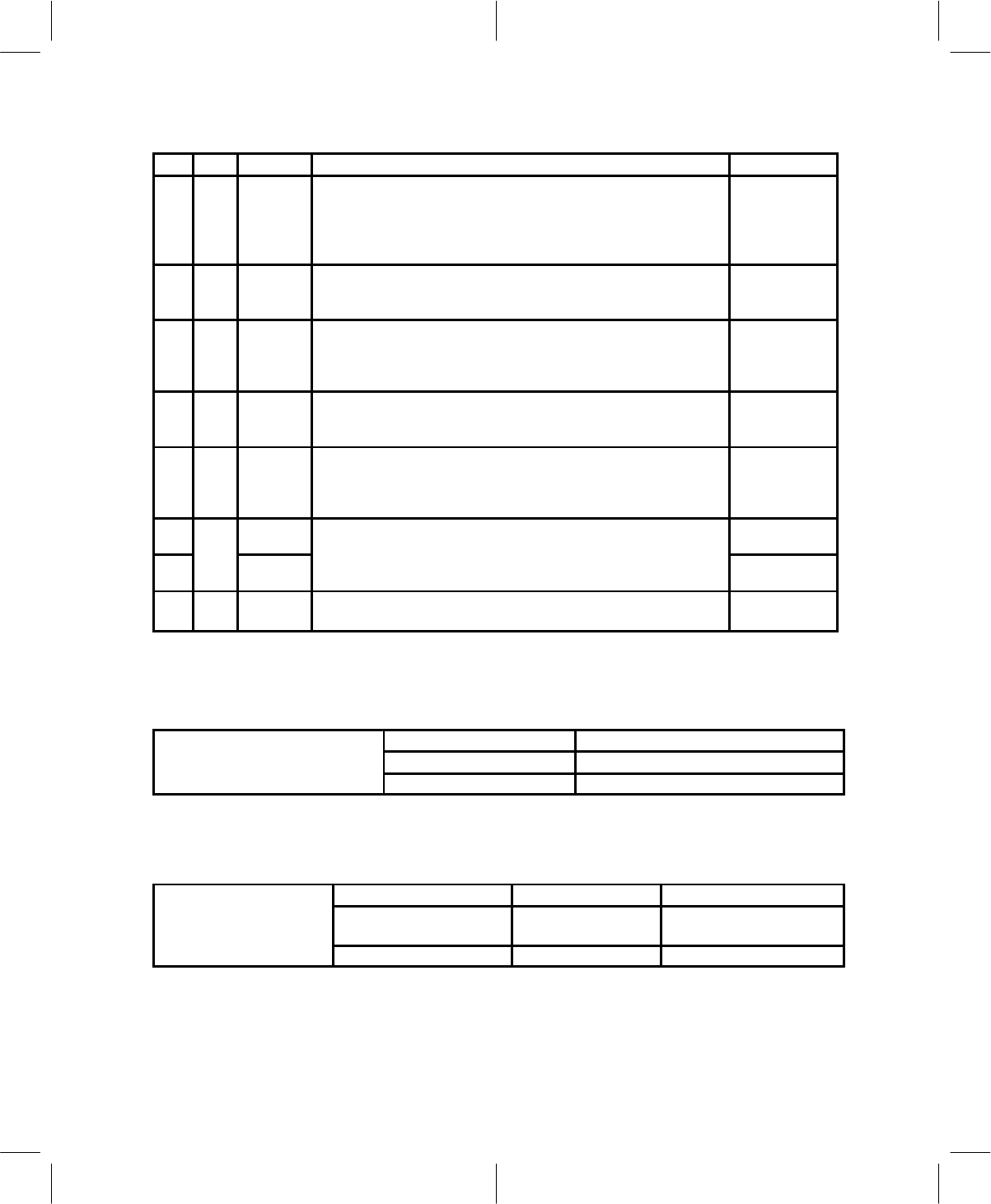
Table 4–19. MStatCtrl Register Bits
BIT R/W NAME FUNCTION RESET VALUE
7 R SYNOL
Synthesizer out of lock. SYNOL is equal to the level applied to SYNOL
input pin. SYNOL can be used as an input for an externally generated
status signal to prevent transmission when external synthesizers are
out of lock. In digital mode, when SYNOL is high, PAEN is not asserted
and no signal can be transmitted from TXIP, TXIN, TXQP, and TXQN.
Level on
SYNOL input
terminals
6 R TXONIND
Transmitter on indicator. TXONIND is equal to the level applied to
TXONIND, and it can indicate that power is applied to the power
amplifier.
Level for
TXONIND input
terminals
5 R SYNRDY
Synthesizer interface ready. SYNRDY indicates that frequency
synthesizer is ready to be programmed by the microcontroller. When
SYNRDY is 1, the microcontroller can program the frequency
synthesizer interface; a 0 indicates the interface circuit is busy.
1
4 R/W MCLKEN
MCLKOUT enable. When MCLKEN is set to 1 by the microcontroller,
the 38.88-MHz master clock is output at MCLKOUT. Writing 0 to
MCLKEN disables MCLKOUT.
1
3 R CVRDY
Conversion ready. A 1 indicates that the latest RSSI or battery voltage
A/D conversion is complete and can be read from the RSSI or battery
register location. CVRDY goes to 0 when the microcontroller reads from
either of these locations.
1
2
R/W
AuxFS[1]
Auxiliary DACs full-scale select. The auxiliary DACs are AGC, AFC,
PWRCONT and also LCD CONTR DAC. The microcontroller selects
0
1
R/W
AuxFS[0]
PWRCONT and also LCD CONTR DAC. The microcontroller selects
the full-scale output ranges with these bits (see Table 4–11 and
Table 4–12 for bit-to-output range mapping).
0
0 R/W MPAEN
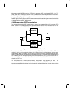
Microcontroller PA enable. A 0 indicates that the external PA enable line
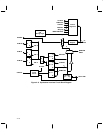
PAEN is prevented from going active (see Figure 4–9).
0
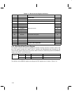
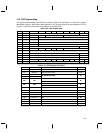
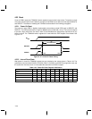
TXI Offset and TXQ Offset: These registers allow the differential offset voltages TXIP – TXIN and
TXQP – TXQN to be adjusted to compensate for internal and/or external offsets. The magnitude of
adjustment is D × step size, where D is a 6-bit, 2s-complement integer written into bits 5–0 of these registers,
as shown here:
TXI(Q) Off
7–6 5–0
TXI(Q) Offset
Reserved TXI(Q) Offset Value
()
W
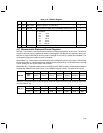
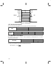
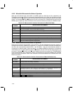
4.18 LCD Contrast
The LCD contrast register allows for 16 levels of control of terminal LCD contrast. The register is input to
the LCD contrast D/A converter allowing control of the level of intensity of the LCD display as shown here:
LDC D/A
7–4 3–1 0
LDC D/A
LCD Contrast Reserved
LCDEN
(active low)
W W