


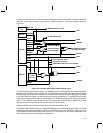

4–27
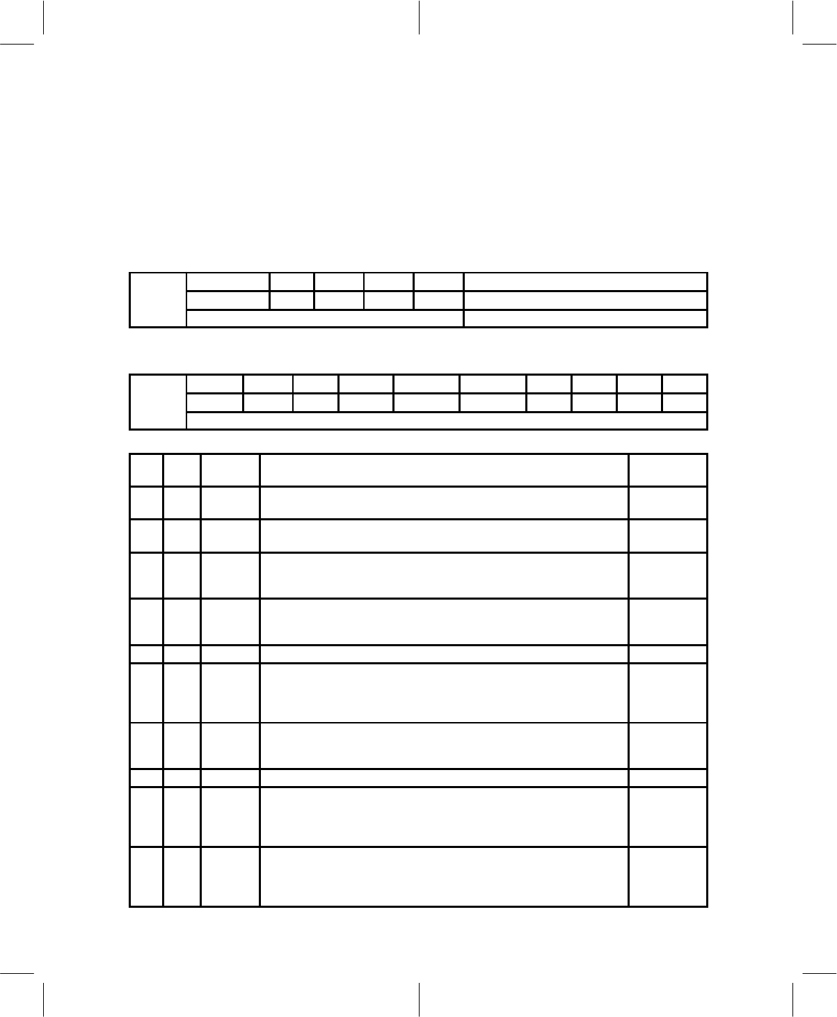
4.22 DSP Status and Control Registers
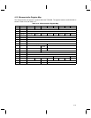
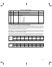
DIntCtrl, Clear and Send Bits: The bit names in the DIntCtrl register indicate the action to be taken when
a 1 is written to the respective bit. When these bits are being read, a 1 indicates that the corresponding
interrupt is pending. A 0 indicates that the interrupt is not pending. Writing a 0 to any bit has no effect. Writing
a 1 to the clear bits clears the corresponding interrupt, and the interrupt terminal returns to its inactive level.
Writing a 1 to the send bits causes the corresponding interrupt to go active.
DIntCtrl, SDIS: When a 1 is written to the SDIS bit, the SINT interrupt going to the DSP is disabled. The
disabling and re-enabling function is buffered to prevent the SINT signal from having shortened periods of
output active. The SDIS bit is active (1) upon reset.
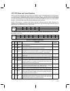
Dl C l
9 8 7 6 5 4–0
DlntCtrl
Clear WBD SDIS Clear-C Send-D Send-F Reserved
R/W
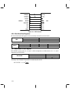
The DStatCtrl register contains various signals needed for system monitoring and control. These are
described in Table 4–22.
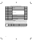
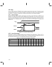
DS C l
9 8 7 6 5 4 3 2 1 0
DStatCtrl
TXGO MODE SCEN FMVOX FMRXEN IQRXEN TXEN OUT1 RXOF ALB
R/W
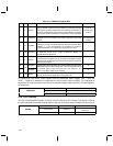
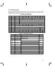
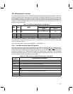
Table 4–22. DStatCtrl Register Bits
BIT R/W NAME FUNCTION
RESET
VALUE
9 R/W TXGO
Transmitter go. TXGO is used in digital mode to initiate (1) and terminate
(0) a transmit burst.
0
8 R/W MODE
Digital (1) – Analog (0) mode select. MODE affects the clock dividers and
the transmitter modes of operation and the Q side filter.
0
7 R/W SCEN
Speech codec enable (microphone/speaker interface chip). SCEN is
connected to bits. SCEN also enables (1) or disables (0) the internal
speech codec clock generation circuits (2.048 MHz – 8 kHz outputs).
0
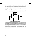
6 R/W FMVOX
FM voice enable. When FMVOX is 1 it enables the Q side of the internal
receiver circuits and connects the receivers Q channel input to FM (see
Figure 4–9).
0
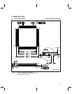
5 R/W FMRXEN FM receiver enable. FMRXEN is connected to bit 5 (see Figure 4–9). 0
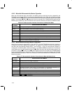
4 R/W IQRXEN
I and Q receiver enable. The IQRXEN is connected to bit 4. When IQRXEN
is 1, it enables (1) power to the I and Q sides of the internal receiver circuits,
and when IQRXEN is 0, it disables (0) power to the I and Q sides of the
internal receiver circuits (see Figure 4–9).
0
3 R/W TXEN
Transmitter enable. TXEN is connected to bit 3. When TXEN is 1, it enables
(1) power to the internal transmitter circuits and when TXEN is 0, it disables
(0) power to the internal transmitter circuits (see Figure 4–9).
0
2 W OUT1 Output 1. OUT1 is a user-defined general purpose data or control signal. 0
1 R/W RXOF
Receive channel offset. When RXOF = 1, it disconnects the RXIP, RXIN,
RXQP, and RXQN terminals from receive channel, and shorts internal
RXIP to RXIN and RXQP to RXQN. It provides the capability of measuring
the dc offset of the receive channel.
0
0 R/W ALB
Analog loop-back. When ALB = 1, it disconnects the RXIP, RXIN, RXQP,
and RXQN terminals from the internal receive channels and connects the
corresponding internal signals to attenuated copies of the TXIP, TXIN,
TXQP, and TXQN signals. The attenuation factor is 8.
0