4–15
4.12 Frequency Synthesizer Interface
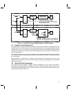
The synthesizer interface provides a means of programming three synthesizers. The synthesizer-side
outputs are a data line, a clock line, and three latch enable lines that separately strobe data into each
synthesizer. The control inputs are registers mapped into the microcontroller address space. The status of
the interface can be monitored to determine when the programming operation has been completed.
The synthesizer interface is designed to be general purpose. Most of the currently available synthesizers
can be accommodated by programming the interface according to the required synthesizer data and logic
level formats.
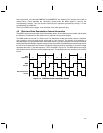
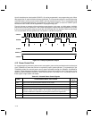
The output of the synthesizer interface consists of five signals. SYNCLK is the common data clock for all
attached synthesizer chips. The clock rate is MCLK/128 (≈304 kHz). The clock pulse has a 50% duty factor.
The serial data output SYNDTA is common to all synthesizers. Three strobe signals, SYNLE0, SYNLE1,
and SYNLE2, are provided. There is one for each synthesizer chip. The attributes of this interface are
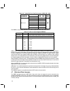
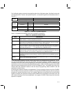
controlled by means of the synthesizer control registers, SynCtrl0, SynCtrl1, and SynCtrl2. These attributes
determine:
• The polarity of the clock (rising or falling edge)
• Whether data is shifted left or right
• The number of bits sent to the synthesizer
• The timing and polarity of the latch enable bits
• The selection of which synthesizer to program
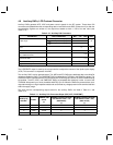
Programming of the synthesizers is accomplished by writing to four microcontroller-mapped data registers.
These registers are chained to form a 32-bit data shift register that can be operated in either shift left or shift
right mode. This register set can accommodate various formats of synthesizer control data. When fewer
than 32 bits of data are to be transmitted, the significant data bits must be justified such that the first bit to
be transferred is either the LSB or the MSB of the register set, as defined by the control register for LSB or
MSB first operation. All 32 bits of the data register are transmitted each time (see Section 4.15 for register
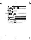
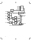
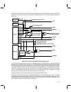
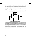
location and Figure 4–6 for a representative block diagram of the frequency synthesizer interface).


